

Pixel structure using voltage programming-type for active matrix organic light emitting device
- Summary
- Abstract
- Description
- Claims
- Application Information
AI Technical Summary
Benefits of technology
Problems solved by technology
Method used
Image

Examples
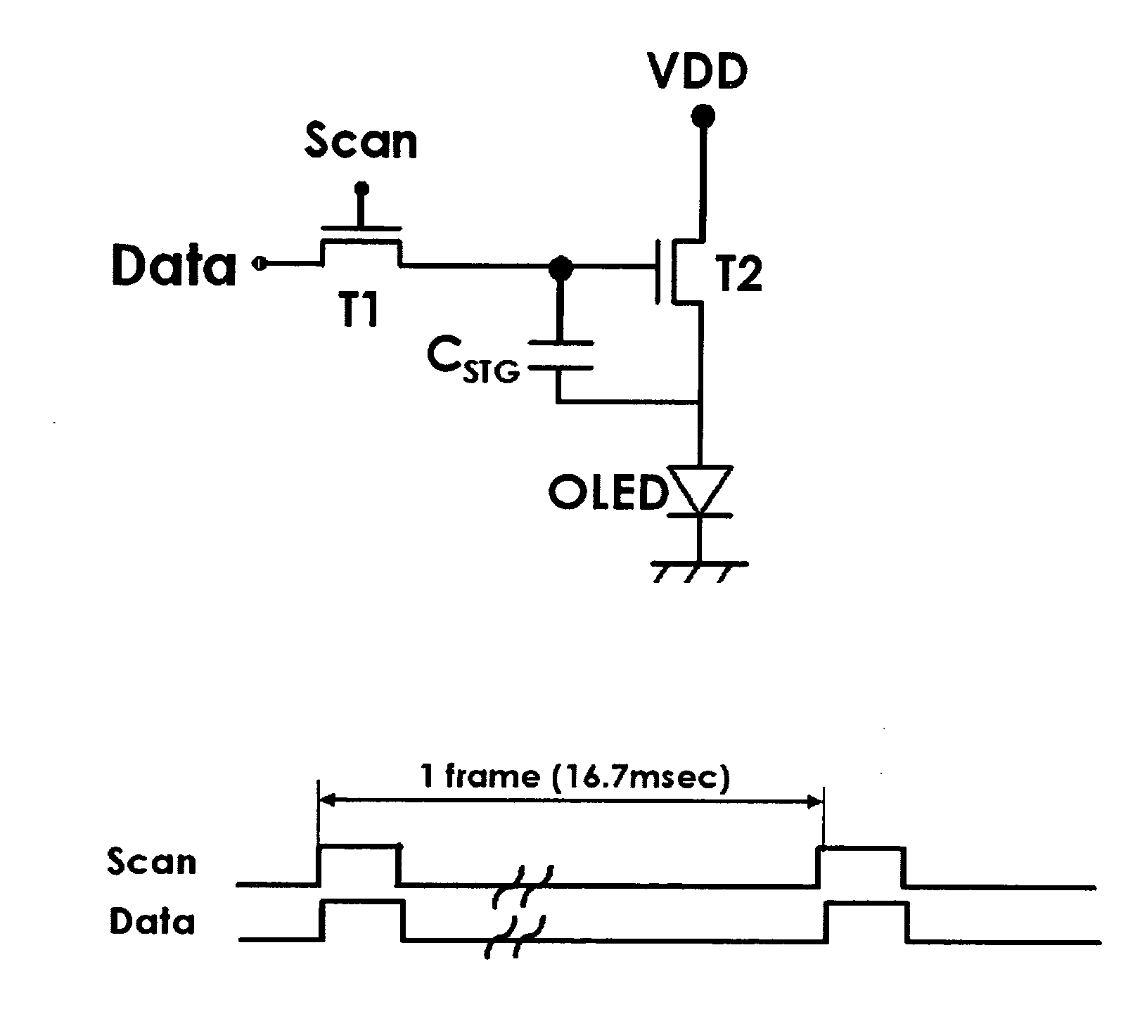
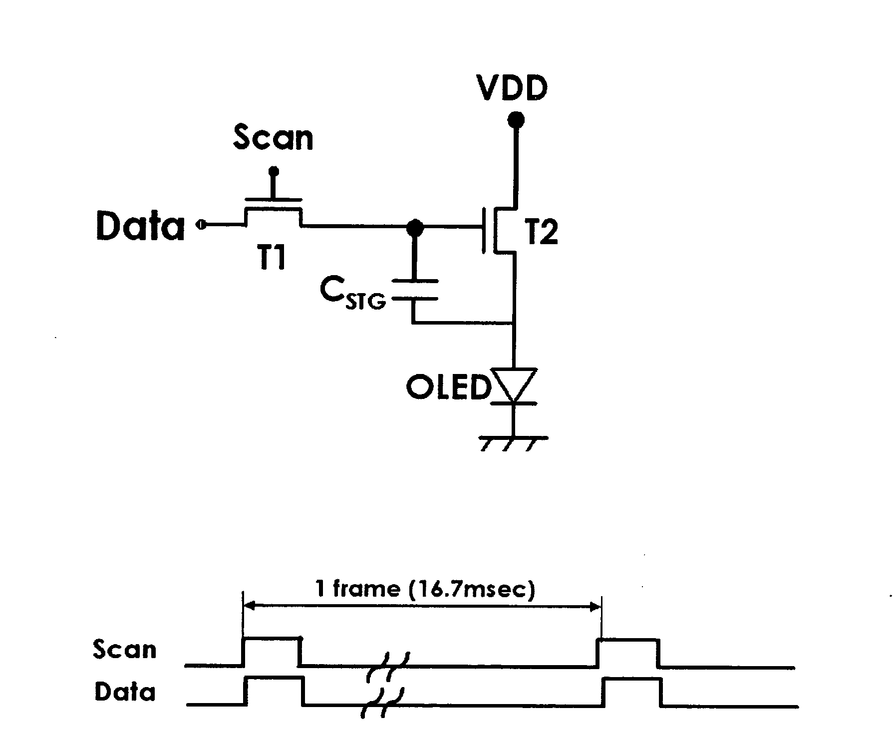
first embodiment
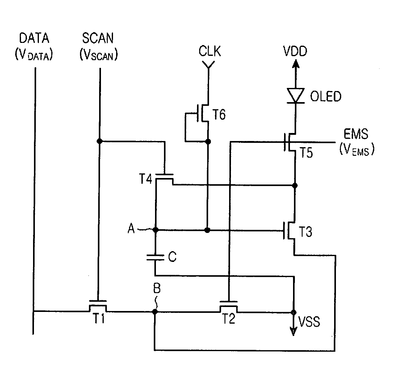
[0030] The operation of the unit pixel as constructed above according to the present invention will be explained. In a period (1) of FIG. 4 where two control signals, i.e., the external management signal EMS and the scan signal SCAN, are all turned on, the fifth TFT T5 and the fourth TFT T4 connected to the third TFT T3 (e.g., driving TFT) are turned on, and the high voltage VDD is pre-charged in the gate node of the third TFT T3 through a diode connection of the third TFT T3 through the fifth TFT T5, to compensate for the threshold voltage of the third TFT T3. In a period (2) of FIG. 4 where the EMS signal goes to a low level and the SCAN signal is in an on state, the current path between the OLED and the third TFT T3 is removed due to the low voltage of the EMS signal, and simultaneously, the gate and the drain of the third TFT T3 are in a diode connection state. In this case, the third TFT T3 operates in a saturation region, and after a predetermined amount of time elapses, the v...
third embodiment
[0035] The operation of the unit pixel according to the present invention will be explained. In a period (1) of FIG. 8 where two control signals, i.e., the external management signal EMS and the scan signal SCAN, are all turned on, the fifth TFT T5 and the fourth TFT T4 connected to the third TFT T3 (e.g., driving TFT) are turned on, and the high voltage VDD is pre-charged in the gate node of the third TFT T3 through a diode connection of the third TFT T3 through the fifth TFT T5, to compensate for the threshold voltage of the third TFT T3. In a period (2) of FIG. 8 where the EMS signal goes to a low level and the SCAN signal is in an on state, the current path between the OLED and the third TFT T3 is removed due to the low voltage of the EMS signal, and simultaneously, the gate and the drain of the third TFT T3 are in a diode connection state. In this case, the third TFT T3 operates in a saturation region, and after a predetermined amount of time elapses, the voltage VGS of the thi...
fourth embodiment
[0038]FIG. 9 is a circuit diagram of a unit pixel of a voltage programming type active matrix OLED according to the present invention, and FIG. 10 is a timing diagram explaining the operation of the unit pixel of FIG. 9. The unit pixel of the voltage programming type active matrix OLED having the construction as illustrated in FIG. 9 is composed of four N-type TFTs and a capacitor. Although the scan signal SCAN and the data signal DATA, which are essential signals for the pixel, are used, the VDD line that is the power supply line is replaced by a VEMS signal line by applying the voltage VEMS to the gate node of the second TFT T2 and the anode of the OLED.
[0039] The operation of the unit pixel according to the fourth embodiment of the present invention will be explained. In a period (1) of FIG. 10 where two control signals, i.e., the external management signal EMS and the scan signal SCAN, are all turned on, a high voltage VEMS connected in series to the OLED is pre-charged in the g...
PUM
 Abstract
Description
Claims
Application Information