Semiconductor device with non-volatile memory and random access memory

a semiconductor device and non-volatile memory technology, applied in the direction of memory adressing/allocation/relocation, digital storage, instruments, etc., can solve the problems of cellular phone functionalities, difficult to give a large capacity to nor flash memory, and require larger capacity memories

Inactive Publication Date: 2005-10-04
RENESAS ELECTRONICS CORP
View PDF10 Cites 50 Cited by
  • Summary
  • Abstract
  • Description
  • Claims
  • Application Information

AI Technical Summary

Benefits of technology

[0015]In at least one preferred embodiment, the present invention provides a semiconductor device comprising: a non-volatile memory having a first reading time; a random access memory RAM having a second reading time, which is more than 100 times shorter than the first reading time; a circuit that includes a control circuit that is connected to and controls access to both the non-volatile memory and the random access memory; and a plurality of input / output terminals connected to the circuit.
[0016]The control circuit is preferably adapted such that at least part of the data stored in the non-volatile memory (flash memory) is transferred to the DRAM (random access memory) before operation of the device. To write data in the non-volatile memory, the data should be initially written to the RAM and then written to the non-volatile memory from the RAM between access requests from devices located outside the semiconductor device. In addition, the control circuit may be adapted to control such that refreshment of the DRAM is hidden from external when the RAM is a DRAM.

Problems solved by technology

Additionally, the recent enhancement of cellular phone functionalities may also require larger capacity memories.
It has been difficult to give a large capacity to the NOR flash memory.
This has been a problem.
On the contrary, the reading time for outputting the first data becomes about 25 μs to 50 μs, so that those flash memories can not easily match the read access speed of an SRAM.
Large capacity SRAMs are confronted with problems in that the data retention current increases in proportion to an increase in the capacity of the memory and the data retention current increases due to an increase in the gate leakage current.
It has been noted that it is increasingly difficult to reduce the data retention current in larger capacity SRAMs.

Method used


Image

  • Semiconductor device with non-volatile memory and random access memory
  • Semiconductor device with non-volatile memory and random access memory
  • Semiconductor device with non-volatile memory and random access memory

Examples


first exemplary embodiment

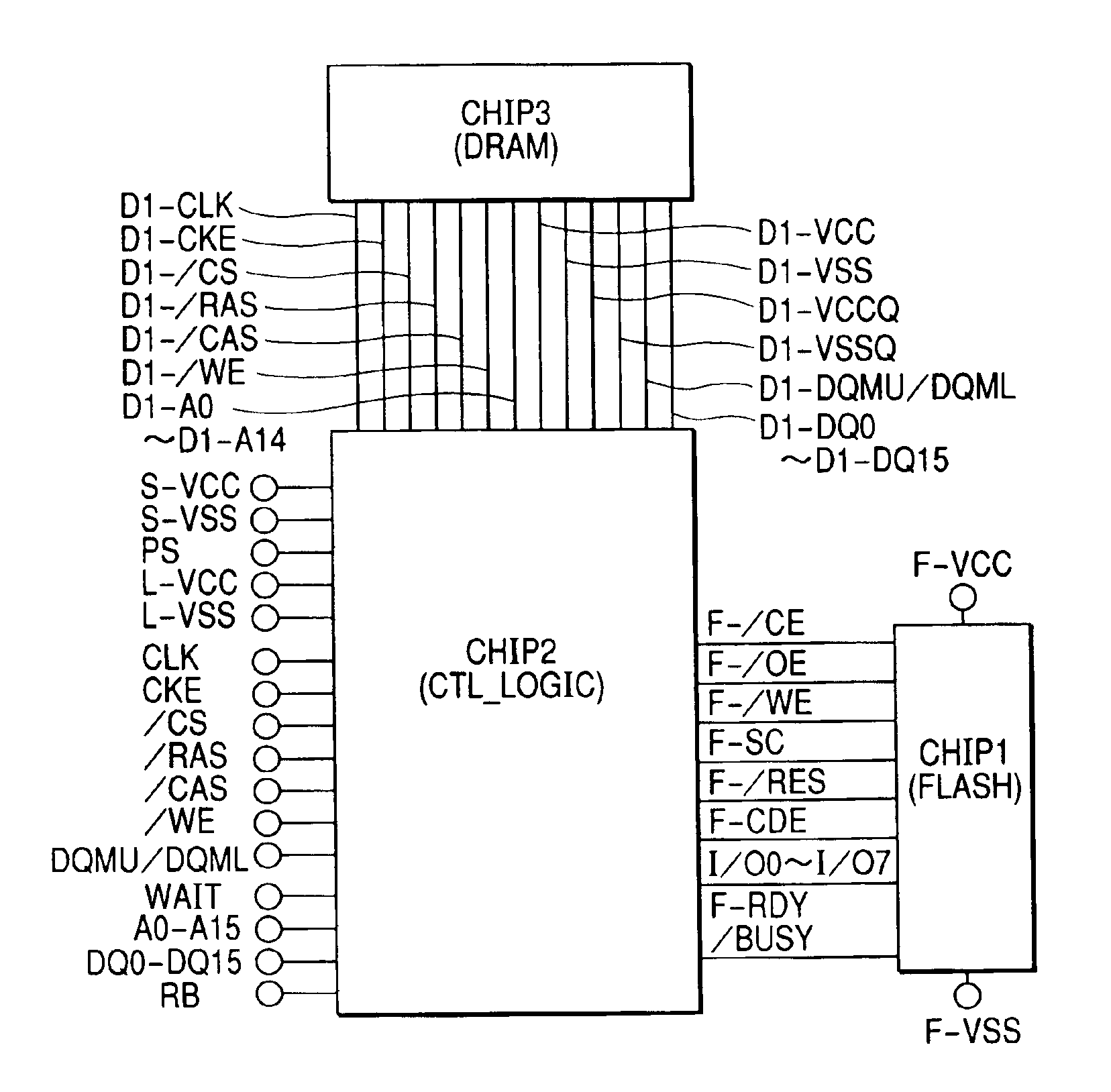
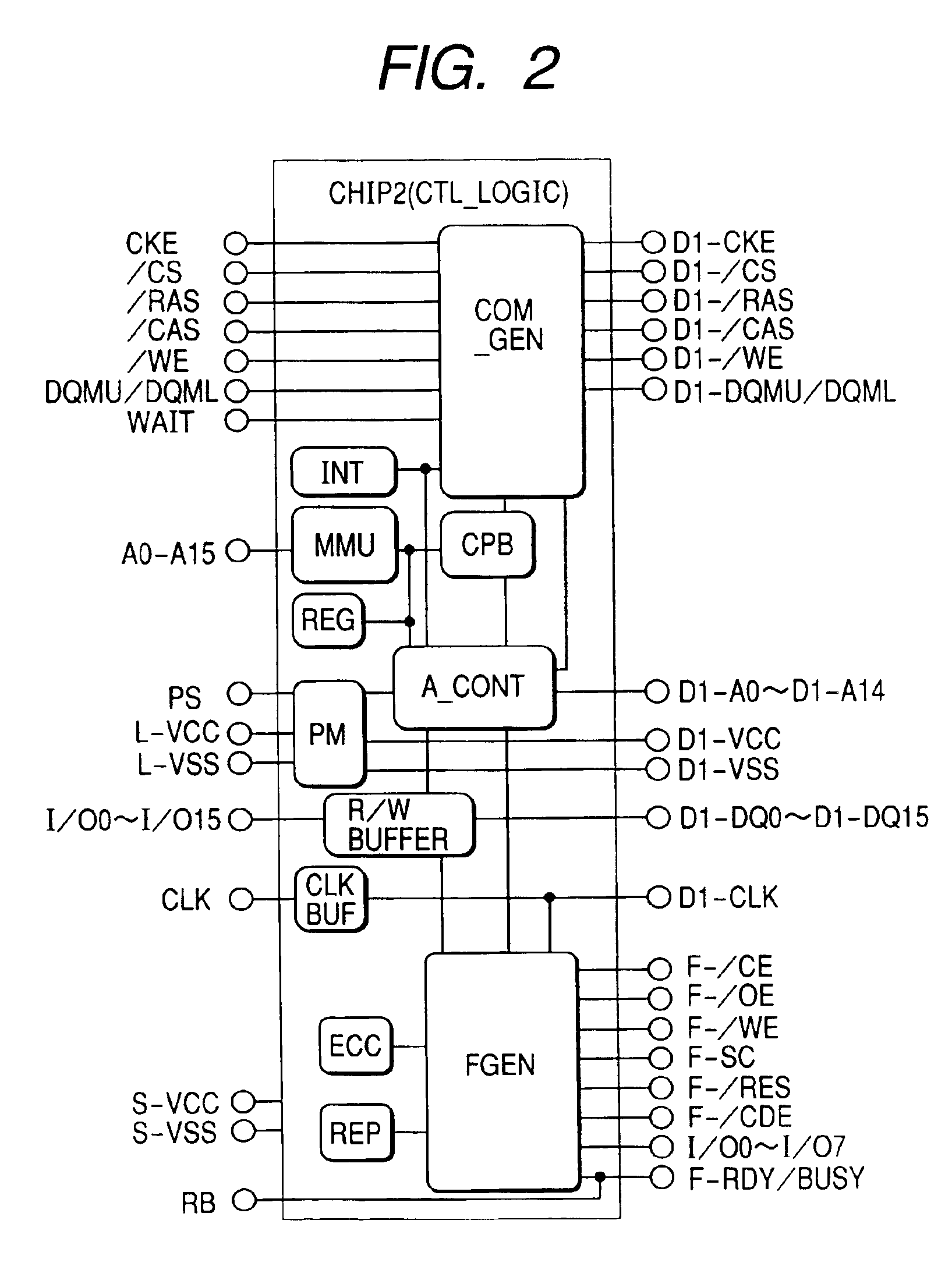
[0065]FIG. 1 shows a first embodiment of a memory module, which is an example of the semiconductor device of the present invention. This memory module is preferably comprised of three chips. Each of those three chips is now described.

[0066]The chip 1 (FLASH) is a non-volatile memory. This non-volatile memory may be a ROM (Read Only Memory), an EEPROM (Electrically Erasable and Programmable ROM), a flash memory, or any similar storage element. A typical example of the non-volatile memory used as chip 1 in this embodiment is a NAND flash memory (to be described below) in the broad sense. The NAND flash memory may have a memory capacity of about 256 Mb and a reading time (time required between a read request and data output) of about 25 μs to 50 μs, which is comparatively slow. On the contrary, the SDRAM used as chip 3 has a large memory capacity of about 256 Mb and a reading time of about 35 ns. Specifically, the reading time of chip 3 is preferably more than 100 times shorter than th...

second exemplary embodiment

[0145]FIG. 21 shows a second exemplary embodiment of the memory module of the present invention. This memory module is comprised of three chips. Hereinafter, each of the three chips will be described in detail. Chip 1 (FLASH) is preferably a non-volatile memory. This non-volatile memory may be a ROM (Read Only Memory), an EEPROM (Electrically Erasable and Programmable ROM), a flash memory, or the like. In this exemplary embodiment, a flash memory is employed. Chip 2 (SRAM+CTL_LOGIC) includes a static random access memory (SRAM) and a control circuit (CTL_LOGIC) that are integrated thereon. The control circuit controls the SRAM integrated on chip 2 as well as chip 3. Chip 3 is a dynamic random access memory (DRAM). The DRAM is classified into various types such as EDO, SDRAM, DDR, etc. according to the differences in the internal configurations and the interface types among them. This memory module may be any of those DRAM types, but the SDRAM is employed in this embodiment as an exa...

third exemplary embodiment

[0225]FIGS. 33A and 33B show a third exemplary embodiment of the memory module of the present invention. FIG. 33A shows a top view and FIG. 33B shows a cross sectional view through line A-A′ of the memory module, respectively. This memory module enables chip 1 (FLASH), chip 2 (CTL_LOGIC), and chip 3 (DRAM) described in the first embodiment or chip 1 (FLASH), chip 2 (SRAM+CTL_LOGIC), and chip 3 (DRAM) described in the second embodiment to be mounted on a substrate (for example, a printed circuit board PCB made of glass epoxy) mounted on an apparatus with use of ball grid arrays (BGA). Although not specifically limited, chip 1 uses a general-purpose DRAM bear chip at one end of which signal and power supply pads are disposed in a line, and chip 3 uses a general-purpose DRAM bear chip in the center of which signal and power supply pads are disposed in a line.

[0226]The bonding pads on chip 1 are connected to the bonding pads on the substrate via bonding wires (PATH2), and the bonding pa...


PUM


Abstract

A semiconductor device including a large capacity non-volatile memory and at least one random access memory, said the access time of said device being matched to the access time of each random access memory. The semiconductor memory device is comprised of: a non-volatile memory FLASH having a first reading time; a random access memory DRAM having a second reading time which is more than 100 times shorter than the first reading time; a circuit that includes a control circuit connected to both the FLASH and the DRAM and enabled to control accesses to those FLASH and DRAM; and a plurality of I/O terminals connected to the circuit. As a result, FLASH data is transferred to the DRAM before the DRAM is accessed, thereby matching the access time between the FLASH and the DRAM. Data is written back from the DRAM to the FLASH as needed, thereby keeping data matched between the FLASH and the DRAM and storing the data.

Description

CLAIM OF PRIORITY[0001]This application is a Continuation application of U.S. application Ser. No. 10 / 164,905 filed Jun. 10, 2002 now U.S. Pat. No. 6,791,877. Priority is claimed based on U.S. application Ser. No. 10 / 164,905 filed Jun. 10, 2002, which claims priority to Japanese Patent Application No. 2001-174978 filed on Jun. 11, 2001.BACKGROUND OF THE INVENTION[0002]1. Field of the Invention[0003]The present invention relates to a stacked memory semiconductor device that includes various kinds of memories, and, more particularly, the present invention relates to a combination of said stacked memories, a method for controlling those memories, and a structure for integrating those memories into a multi-chip module.[0004]2. Description of the Background[0005]The following documents are referenced in this specification. The documents are numbered, and hereinafter, they will be described with reference to these numbers. [“Document 1”]: LRS1337 Stacked Chip 32M Flash Memory and 4M SRAM ...

Claims


Application Information

Patent Timeline
Patent Type & Authority Patents(United States)
IPC IPC(8): G11C11/00G06F12/16G06F3/06G06F12/00G06F12/06G11C5/02G11C8/00G11C11/401G11C11/406G11C11/407G11C11/412G11C16/02G11C16/04G11C16/10G11C16/32
CPCG11C5/02G11C5/025G11C5/04G11C11/005G11C11/406G11C11/40603G11C11/40607G11C11/412G11C16/10G11C16/32G06F12/0246G11C16/26G11C29/70G11C16/0483
Inventor MIURA, SEIJIAYUKAWA, KAZUSHIGE
Owner RENESAS ELECTRONICS CORP
Why Eureka
Try Eureka