On chip network

a chip network and chip technology, applied in the field of on-chip networks, can solve the problems of limited concurrent operation capabilities, limited maximum frequency of operation, and significant performance penalty for the overall system and/or particular processors

Inactive Publication Date: 2004-01-29
NORTH STAR INNOVATIONS
View PDF12 Cites 110 Cited by
  • Summary
  • Abstract
  • Description
  • Claims
  • Application Information

AI Technical Summary

Problems solved by technology

Typical bus architectures, including those listed above, are very similar in structure and share a set of problematic characteristics.
The result is limited concurrent operation capabilities, concurrency between address and data tenures, and concurrency between read and write data tenures.
These handshakes can limit the maximum frequency of operation.
SOC designs often required two or more different processor types, which were incompatible and not designed to directly communicate with each other.
It was possible to use existing bus structures, but this resulted in a significant performance penalty for the overall system and / or particular processors.
The existing switch fabric architectures, however, were complicated and expensive to integrate onto a single chip.

Method used


Image

  • On chip network
  • On chip network
  • On chip network

Examples


Embodiment Construction

[0024] As used herein, the terms "assert" and "negate" are used when referring to the rendering of a signal, status bit, or similar apparatus into its logically true or logically false state, respectively. For positive logic, the logically true state is a logic level one (1) and the logically false state is a logic level zero (0). And for negative logic, the logically true state is a logic level zero and the logically false state is a logic level one. Signal names conform to positive logic. A number with a "b" appended thereto indicates that the number is represented in binary format. A number with an "h" appended thereto indicates that the number is represented in hexadecimal format. A number without an appended letter indicates decimal unless otherwise specified.

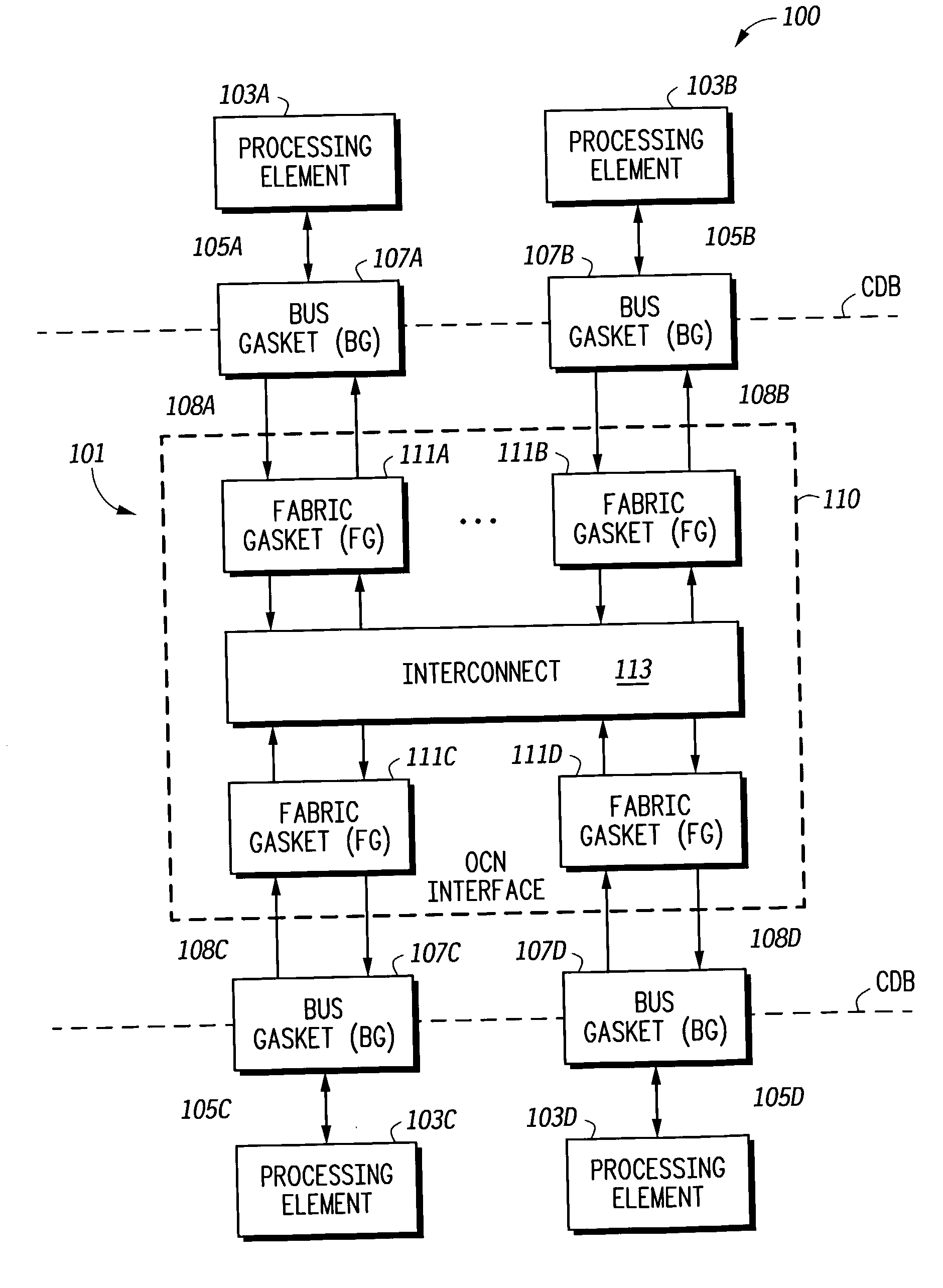
[0025] FIG. 1 is a simplified block diagram of an on chip communication system 100 including an on chip network (OCN) 101 implemented according to an embodiment of the present invention that enables communication among one...


PUM


Abstract

An OCN for integrated processing elements including a network with multiple ports and multiple port interfaces. The ports and the port interfaces conform to a consistent port protocol. Each port interface converts information between bus transactions of a corresponding processing element and network packets and exchanges network packets with other port interfaces. Each port includes an arbitration interface and a data interface and the network includes an interconnect and an arbiter. The interconnect includes selectable data paths between the ports for packet datum transfer. A port source interface submits transaction requests and provides packet datums upon receiving an acknowledgement. A port destination interface receives packet datums via available input buffers. Each transaction request includes a transaction size and a destination port address. The arbiter receives transaction requests, arbitrates among transaction requests, provides acknowledgements and controls the interconnect to select data paths between sources and destinations.

Description

[0001] The present invention relates to communications for system on chip (SOC) configurations, and more particularly to a packet-based on chip network (OCN) that enables and manages data operations between multiple processing elements integrated on an integrated circuit (IC) or chip.DESCRIPTION OF RELATED ART[0002] A market trend that has been observed is to provide an increasing number of integrated processing cores on a single chip. An interconnect system must be provided to enable communication between each core. Although the cores may be homogeneous (each of the same type), the interconnect system must often support on-chip communications between heterogeneous processing elements. Current System On Chip (SOC) configurations are designed around shared bus communication mechanisms. These buses are bridges to other shared bus structures. A few examples include IBM's CoreConnect bus, Motorola's 60X bus, ARM's Advanced Microcontroller Bus Architecture (AMBA), and the industry standa...

Claims


Application Information

Patent Timeline
Patent Type & Authority Applications(United States)
IPC IPC(8): H04L12/56
CPCH04L49/101H04L49/102H04L49/30H04L49/254H04L49/109
Inventor GARINGER, NED D.DORR, MARTIN L.NAUMANN, MARK W.WALKER, GARY A.
Owner NORTH STAR INNOVATIONS
Why Eureka
Try Eureka