
Chip package substrate having soft circuit board and method for fabricating the same
a chip package and soft circuit board technology, applied in the direction of printed element electric connection formation, non-printed electric components of printed circuits, radio frequency controlled devices, etc., can solve the problems of reduced installation flexibility of the package body, increased material cost, high price of the ceramic package substrate, etc., to reduce manual operations, improve the yield of the product, and simplify the electric connection process
- Summary
- Abstract
- Description
- Claims
- Application Information
AI Technical Summary
Benefits of technology
Problems solved by technology
Method used
Image

Examples
Embodiment Construction
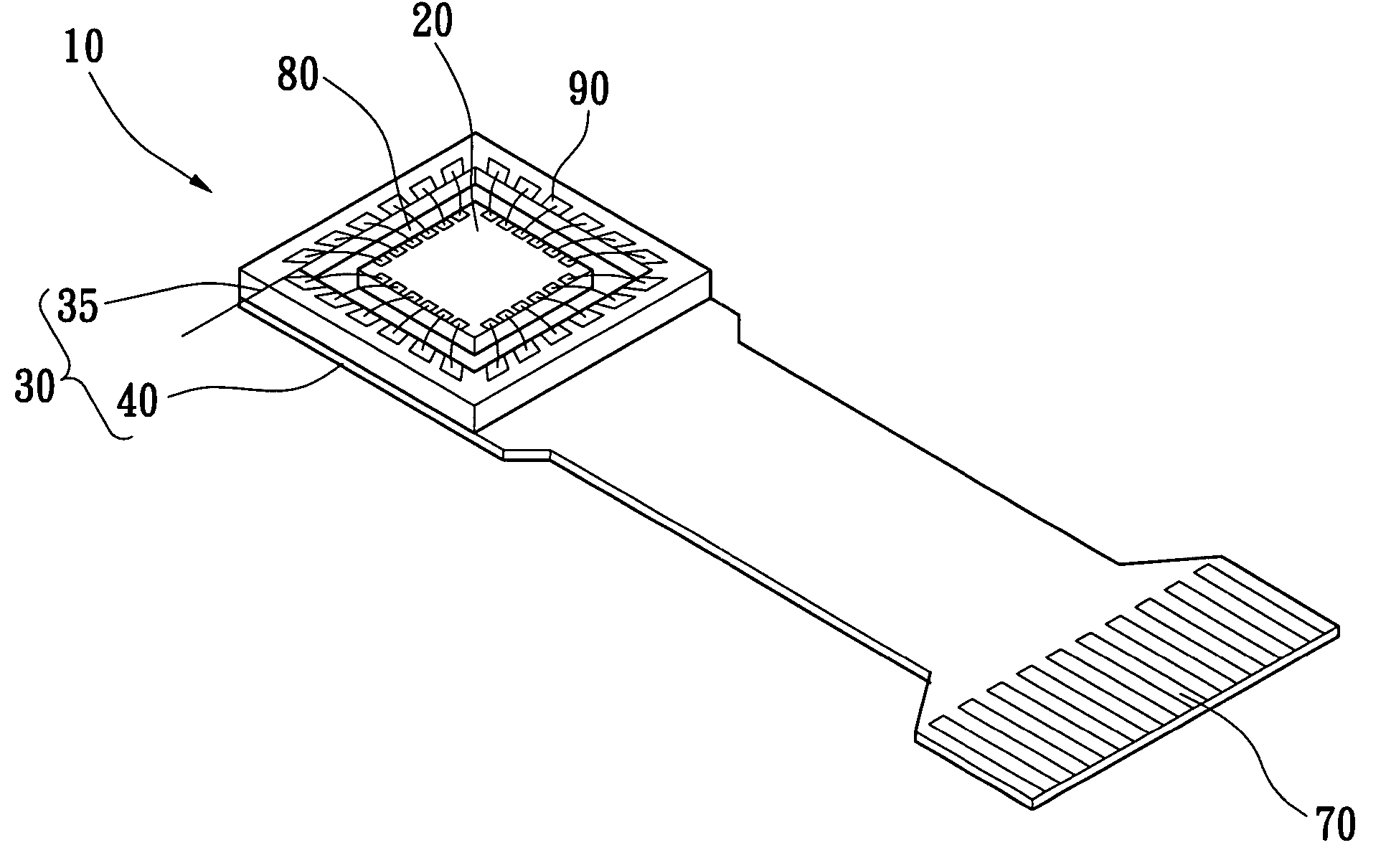
[0022] As shown in FIG. 3, the present invention provides a soft circuit board and a method for manufacturing the same. An image-sensing chip is packaged on the chip package substrate. The soft circuit board is used as external signal connection lines to connect an electronic board for forming an image detection module thereto. The method for manufacturing the chip package substrate having a soft circuit board provides manufacturing of the chip package substrate having a soft circuit board before chip packaging, hence simplifying the adhesion process of the soft circuit board after the chip is packaged on the chip package substrate.
[0023] As shown in FIGS. 3 and 4, a chip package substrate 10 having a soft circuit board is used to package an image-sensing chip 20. The soft circuit board is used as external signal connection lines. The chip package substrate 10 comprises a multi-layer soft and hard composite PCB 30, a plurality of conducting components 50 and a plurality of conducti...
PUM
| Property | Measurement | Unit |
|---|---|---|
| Hardness | aaaaa | aaaaa |
Abstract
Description
Claims
Application Information