Stacked wafer scale package

Inactive Publication Date: 2006-02-23
TEXAS INSTR INC
View PDF9 Cites 86 Cited by
  • Summary
  • Abstract
  • Description
  • Claims
  • Application Information

AI Technical Summary

Benefits of technology

[0003] The problems noted above are solved at least in part by a device comprising high-density, stacked wafer scale packages. In at least some embodiments, the device comprises a first die enclosed in a wafer scale package, said first die

Problems solved by technology

Conversely, a non-wafer scale package is not formed directly onto a die and is often larger than the die, resulting in relatively poor package density, an inefficient use of space and a package that is thus unnecessarily large.
However, because wafer scale packages are b

Method used


Image

  • Stacked wafer scale package
  • Stacked wafer scale package
  • Stacked wafer scale package

Examples


Embodiment Construction

[0017] The following discussion is directed to various embodiments of the invention. Although one or more of these embodiments may be preferred, the embodiments disclosed should not be interpreted, or otherwise used, as limiting the scope of the disclosure, including the claims. In addition, one skilled in the art will understand that the following description has broad application, and the discussion of any embodiment is meant only to be exemplary of that embodiment, and not intended to intimate that the scope of the disclosure, including the claims, is limited to that embodiment.

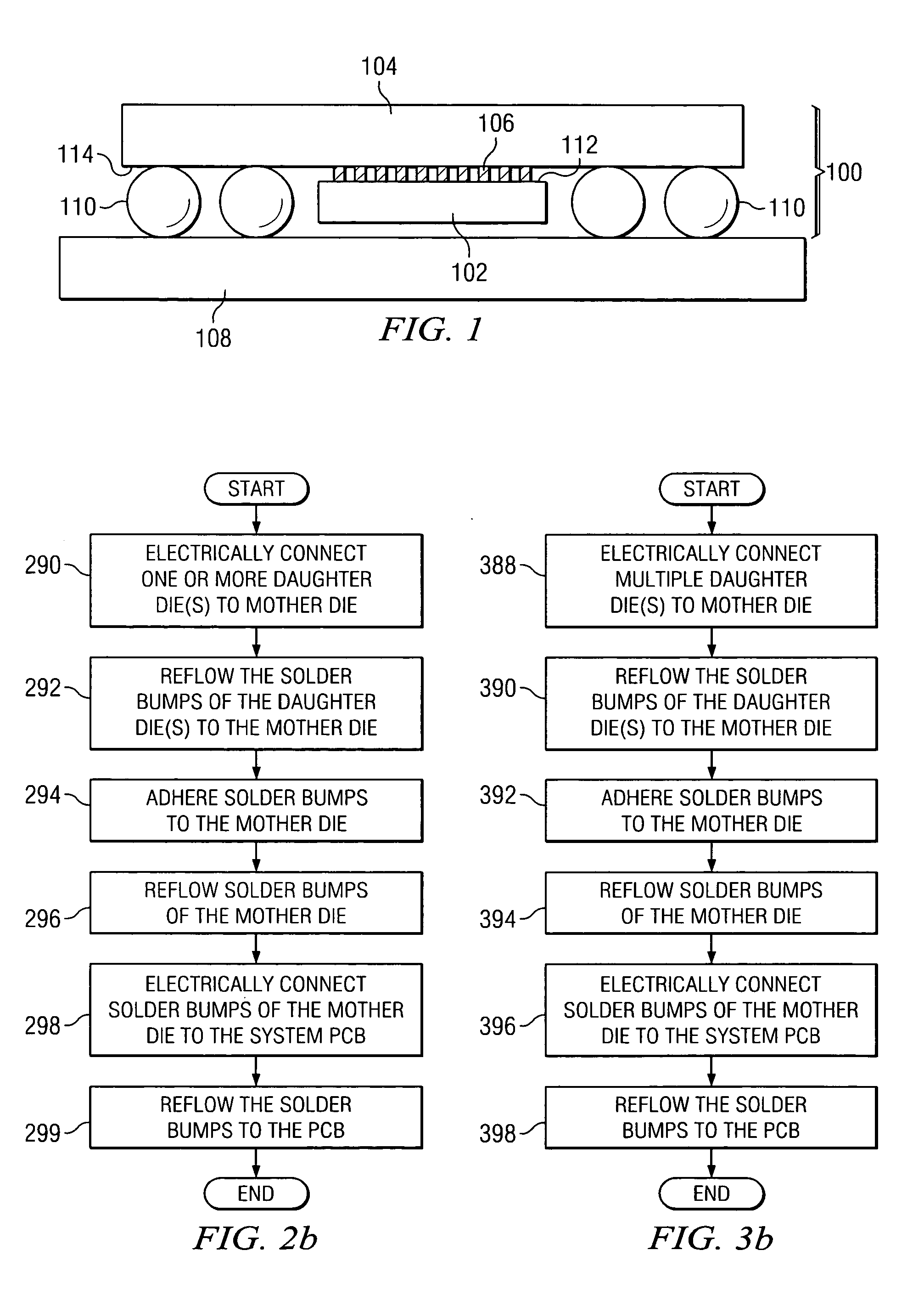
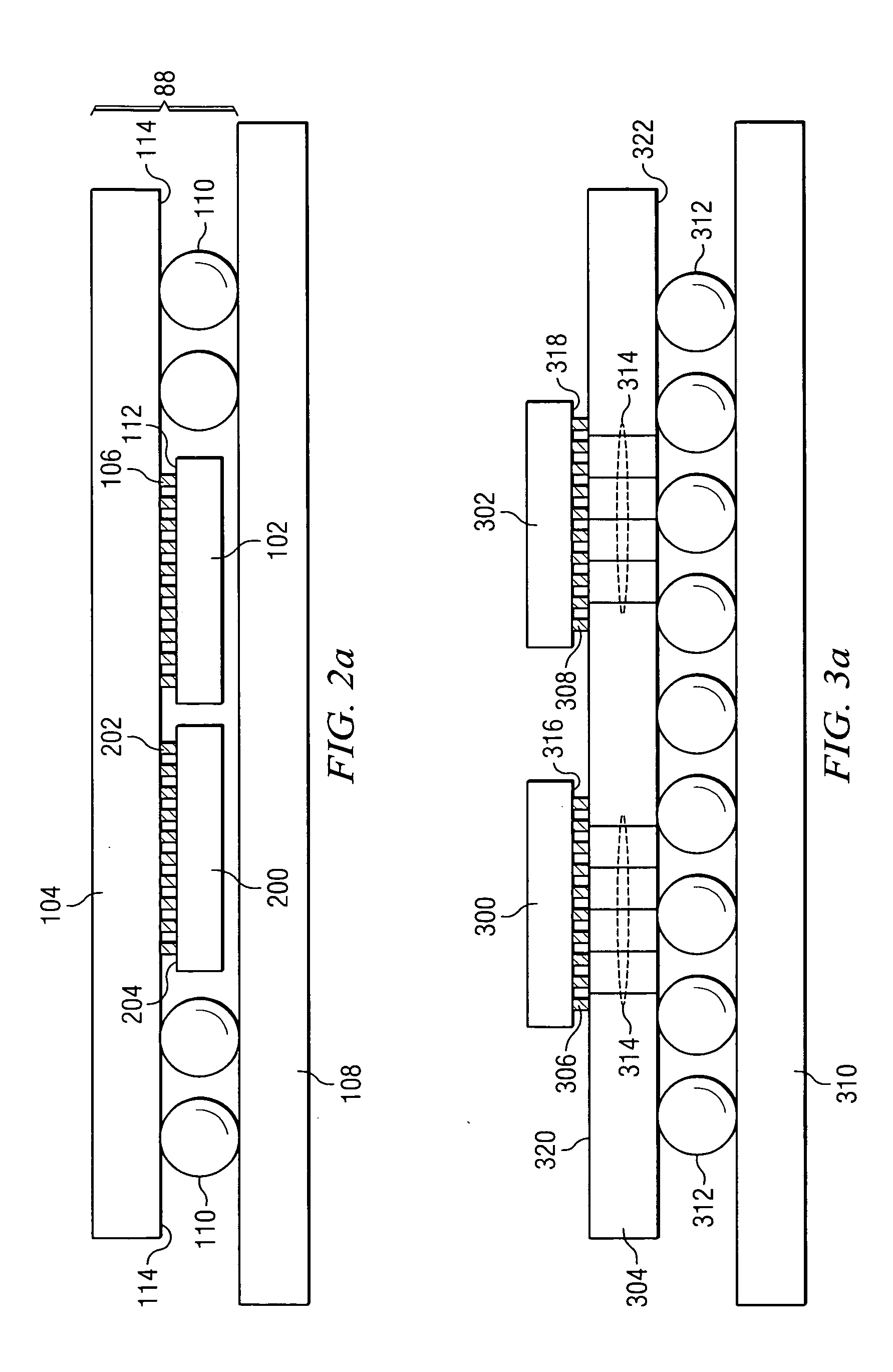
[0018] The physical configuration of a die stack dictates the amount of space the die stack occupies. Accordingly, described herein are various efficient wafer-scale package stacking configurations with circuit densities greater than those produced by traditional, non-wafer scale stacking techniques. FIG. 1 illustrates a daughter die 102 electrically connected to a mother die 104 by way of connections 106...


PUM


Abstract

A device comprising a first die enclosed in a wafer scale package, said first die adapted to mate with a printed circuit board (“PCB”) via solder bumps. The device further comprises a second die enclosed in a wafer scale package and electrically connected to a surface of the first die facing the PCB to form a die stack.

Description

BACKGROUND [0001] In a “stacked die” integrated circuit (“IC”) package, two or more semiconductor dies are electrically connected by arranging each die on top of another die. Stacked die packaging technologies have gradually gained market acceptance for use in mobile phone and handheld device applications, where increased functionality, reduced form factor and lighter weight continue to be substantial driving forces. For example, companies such as Nokia® and Ericsson® regularly introduce mobile phones that are smaller, lighter and more useful than before. IC packages containing stacked dies are desirable because the stacked dies provide substantial functionality while occupying a minimum amount of printed circuit board (“PCB”) space. [0002] A relatively small IC package is the “wafer scale” package. The wafer scale package is formed directly onto a die and generally is the same size as or only slightly larger than the die, resulting in relatively high package density and an efficien...

Claims


Application Information

Patent Timeline
IPC IPC(8): H01L23/02H01L23/52
CPCH01L23/481H01L25/0657H01L2224/16145H01L2224/48145H01L2225/06506H01L2225/06513H01L24/48H01L2225/06541H01L2924/01079H01L2924/14H01L2924/15311H01L2924/1532H01L2225/06517H01L2924/00014H01L2924/181H01L2224/16225H01L2924/00011H01L2224/0401H01L2924/00012H01L2224/45099H01L2224/45015H01L2924/207
Inventor EDWARDS, DARVIN R.
Owner TEXAS INSTR INC
Why Eureka
Try Eureka