Pulse width modulation device with a power saving mode controlled by an output voltage feedback hysteresis circuit

a technology of output voltage feedback and pulse width, which is applied in the direction of pulse generator, pulse manipulation, pulse technique, etc., can solve the problems of wasting power consumption in the condition of light load, working loss includes conduction loss and switching loss, conduction loss decreases, etc., to achieve stable output, save power, and improve efficiency

US20060109039A1Inactive Publication Date: 2006-05-25NIKO SEMICON
8 Cites 35 Cited by

Patent Information

Authority / Receiving Office
US · United States
Patent Type
Applications(United States)
Current Assignee / Owner
Publication Date
2006-05-25
Estimated Expiration
Not applicable · inactive patent

Smart Images

  • Figure 1
    Figure 1
  • Figure 2
    Figure 2
  • Figure 3
    Figure 3
Patent Text Reader

Abstract

A pulse width modulation device with a power saving mode controlled by an output voltage feedback hysteresis circuit is used in a power supply. The present invention comprises a hysteresis comparison circuit extracting a feedback voltage, a high threshold voltage and a low threshold voltage, and the voltages are executed by a comparison and hysteresis operation to a output blanking signal, a PWM control unit extracting a detecting current signal and the feedback voltage to output a modulation signal after a comparison operation is executed; an OR gate circuit connected to the hysteresis comparison circuit and the PWM control unit for receiving the blanking signal and the modulation signal to output a reset signal; and a synchronization signal output unit connected to the OR gate circuit for receiving the reset signal and an oscillation signal to output the drive signal.
Need to check novelty before this filing date? Find Prior Art

Description

BACKGROUND OF THE INVENTION

[0001] 1. Field of the Invention

[0002] This invention relates to a pulse width modulation device with a power saving mode controlled by an output voltage feedback hysteresis circuit. In particular, this invention relates to a pulse width modulation device used in a power supply that controls the output driving signal according to the output load variation.

[0003] 2. Description of Related Art

[0004] In the applications of low power output, such as a charger for a mobile phone, a wireless telephone, a digital still camera and a PDA, and an AC voltage regulator for a printer, a TV game player, and a hand-held Walkman, has great request for power saving in a standby mode.

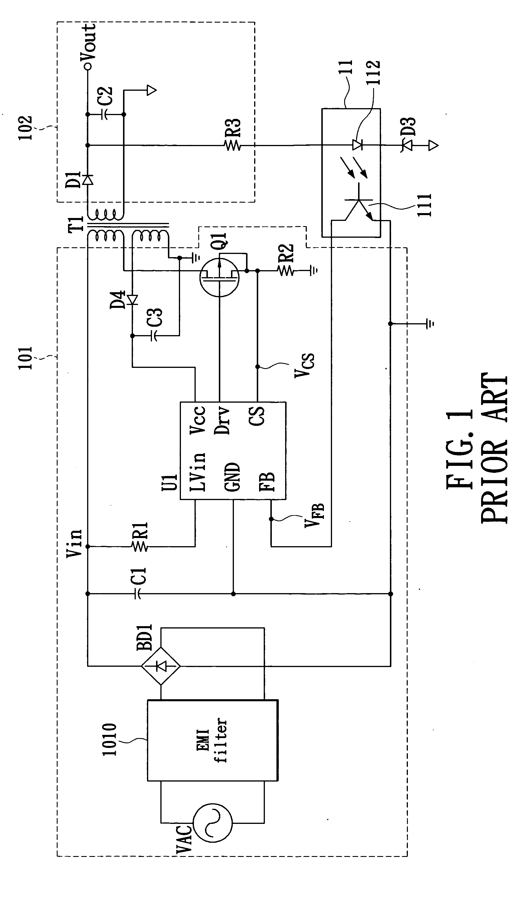
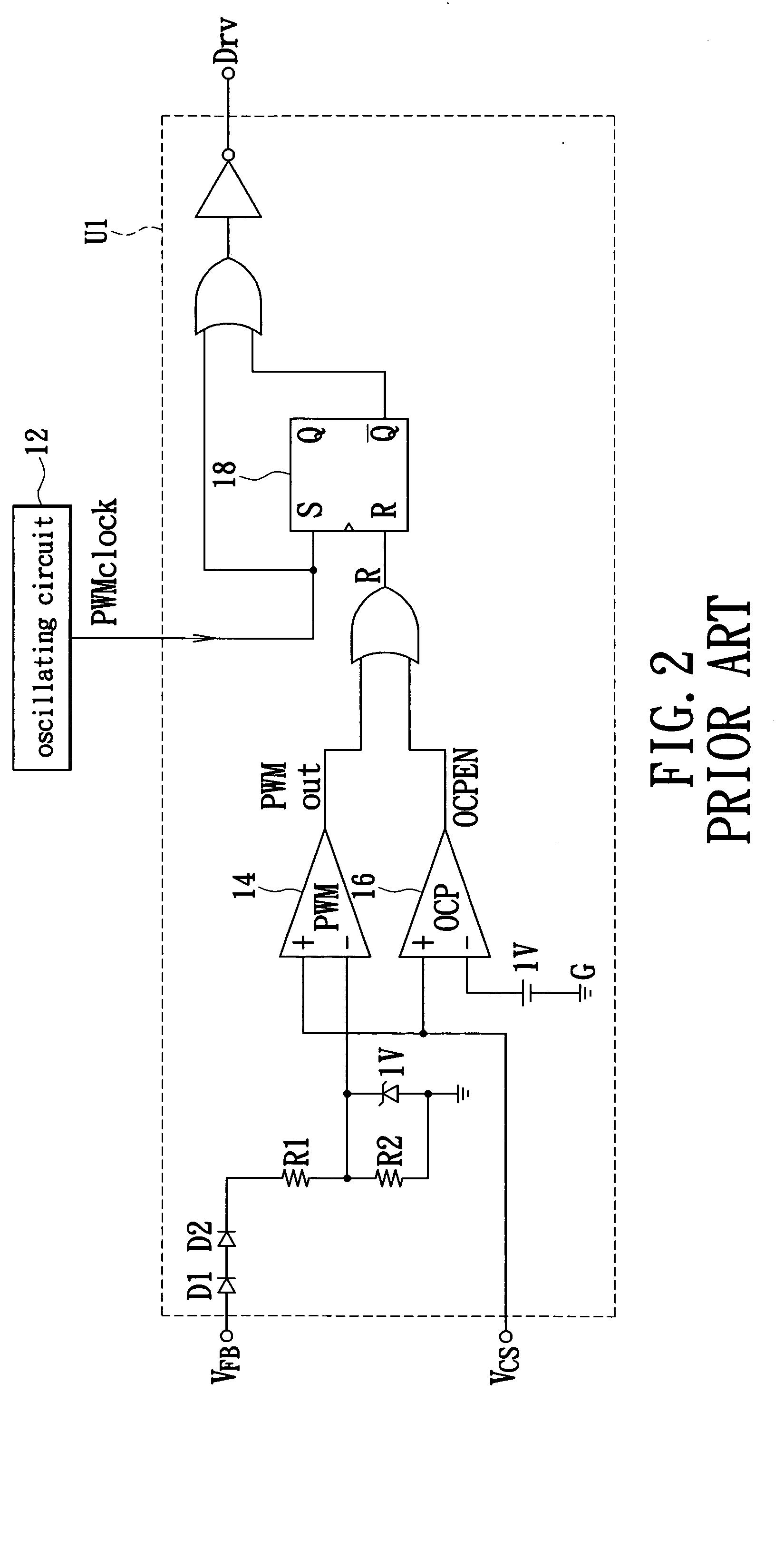
[0005] In currently known DC power supply devices, such as an AC-to-DC switching power supply, in order to reduce the volume of a transformer, a high-frequency pulse width modulation PWM is widely used to control a DC output voltage, as shown in FIG. 1, which is a structure diagram of the ...

Examples

Embodiment Construction

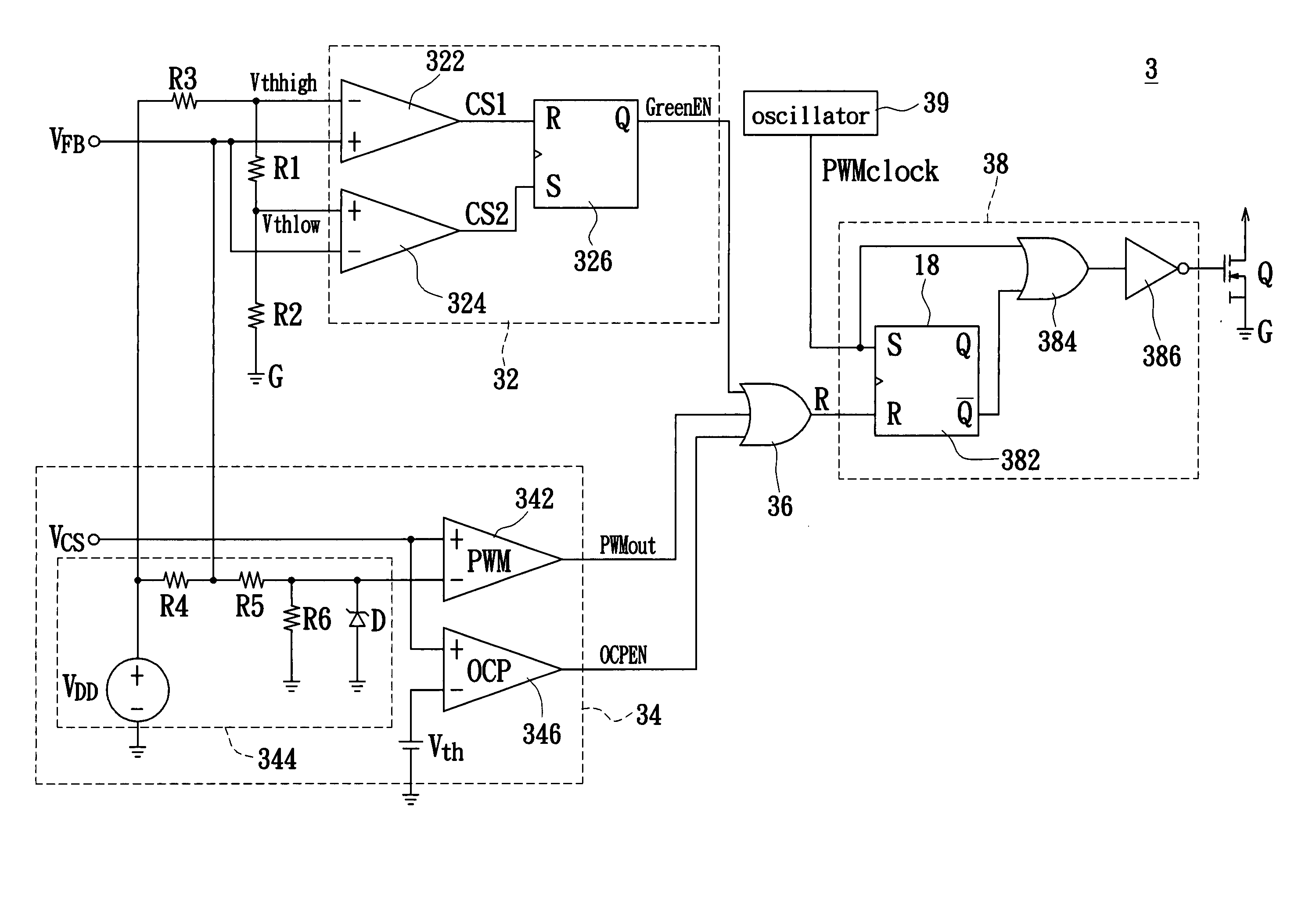
[0024] Please refer to FIG. 5, which shows a schematic view of the circuit of the present invention. A pulse width modulation device 3 of the present invention controls and outputs a drive signal DRV to a power switch Q according to the load variation of a power supply. The pulse width modulation device 3 includes a hysteresis comparison circuit 32, a pulse width modulation control unit 34, a OR gate circuit 36 and a synchronization signal output unit 38.

[0025] Please refer to FIG. 5 again. The pulse width modulation device 3 of the present invention receives a feedback voltage VFB from a load terminal of the power supply and uses a DC power supply VDD to send the electric power to a first resistor R1 and a second resistor R2 that are connected in series via a resistor R3. Then, the voltage of the electric power is divided into a high threshold voltage Vthhigh and a low threshold voltage Vthlow via the two resistors R1 and R2.

[0026] Further, the hysteresis comparison circuit 32 ex...