

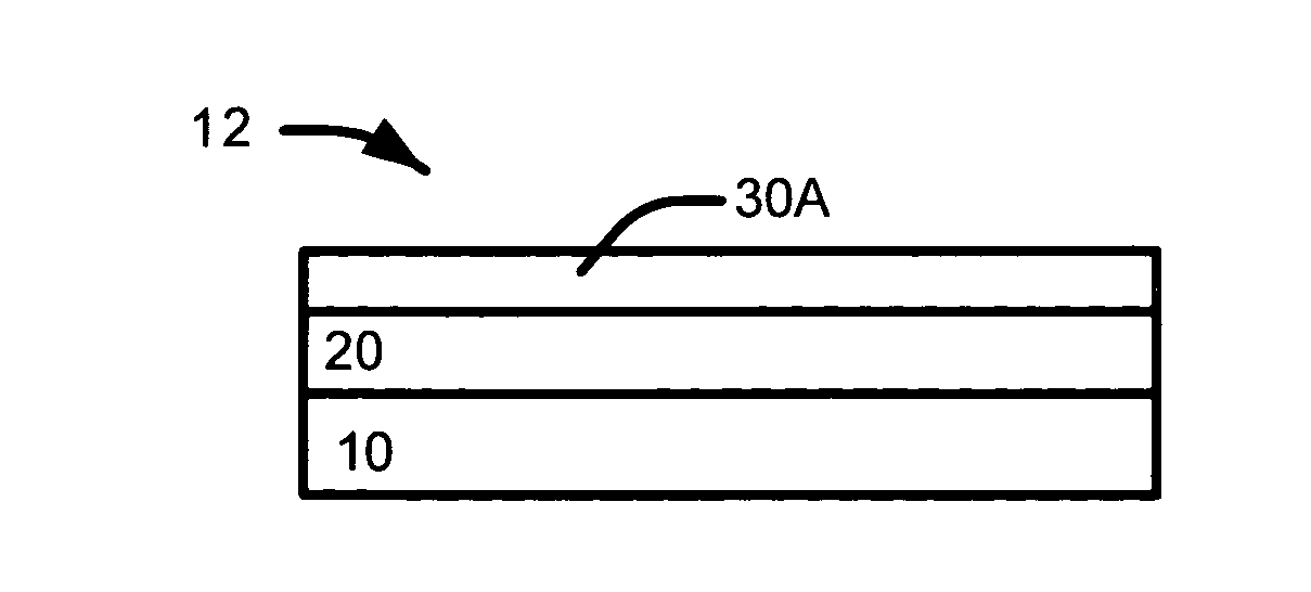
Material architecture for the fabrication of low temperature transistor
a technology of low temperature transistors and materials, applied in the direction of transistors, electric devices, solid-state devices, etc., to achieve the effect of reducing repetition
- Summary
- Abstract
- Description
- Claims
- Application Information
AI Technical Summary
Problems solved by technology
Method used
Image

Examples
example embodiment
III. Overview—General Example Embodiment
[0073] Some example embodiments form a carbon-containing layer in the EOR regions of an implanted (e.g.,) doped region in a silicon containing substrate. The carbon-containing layer and the implanted region can be formed in any order. The carbon-containing layer helps reduce defects from the implant that formed the implanted or doped region.
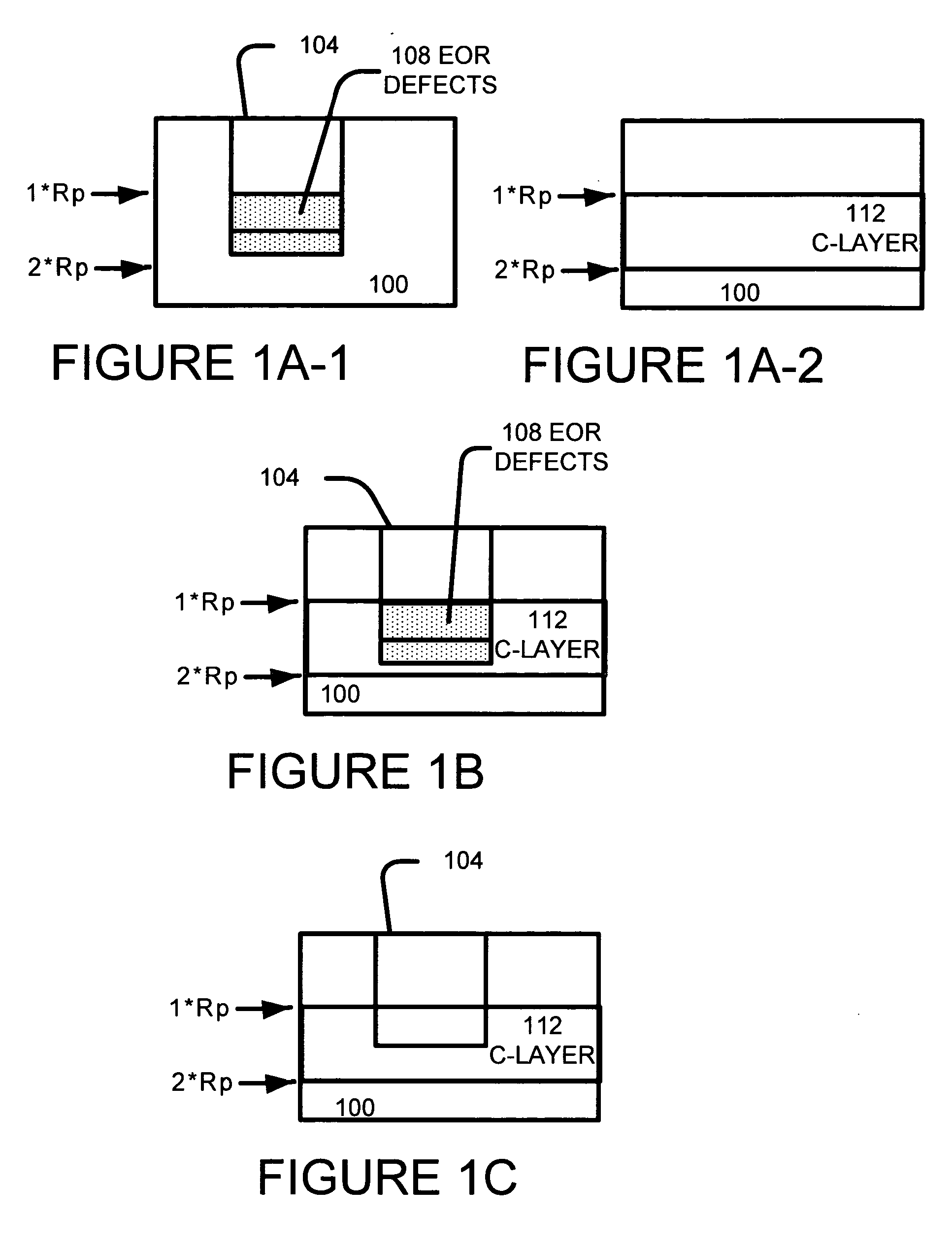
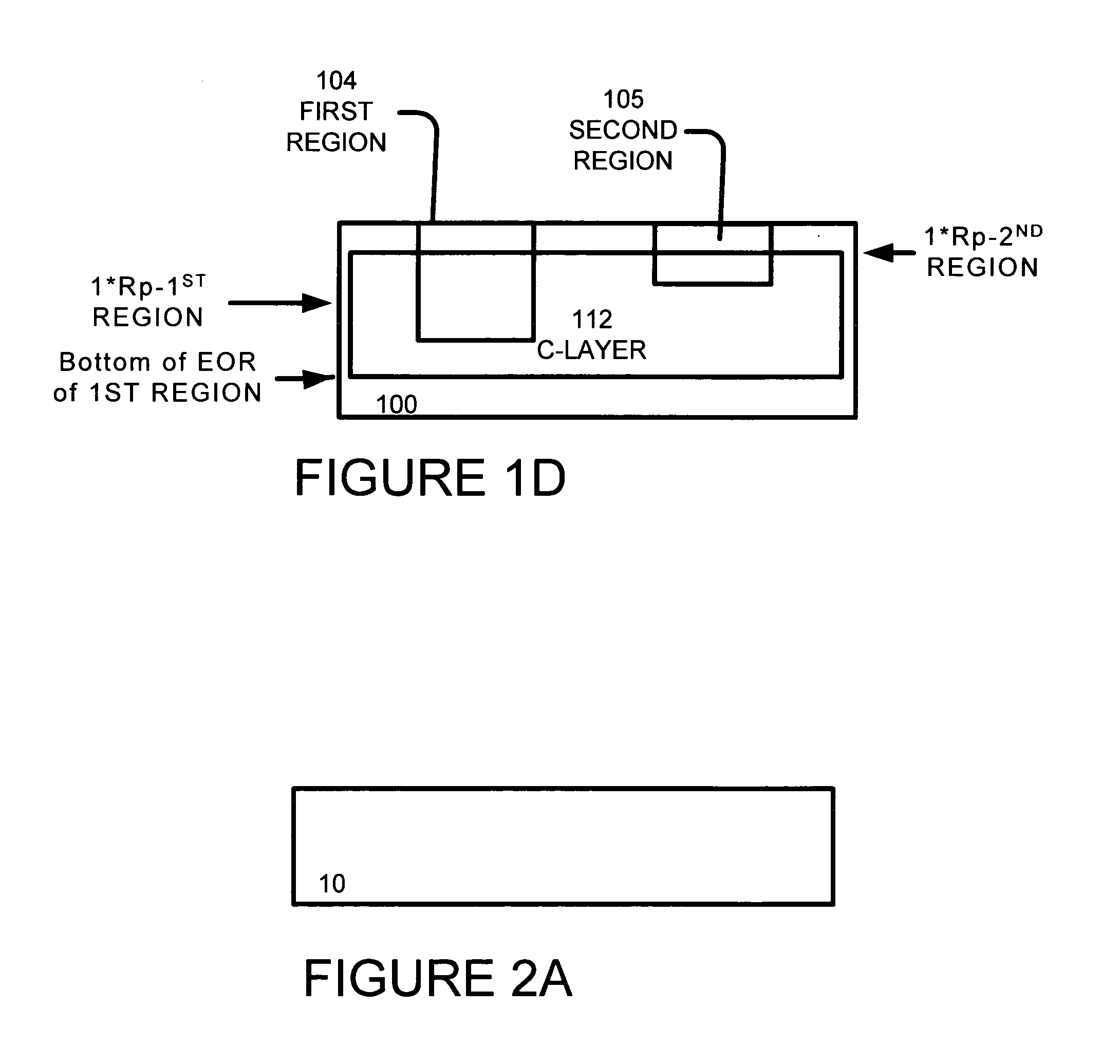
[0074]FIGS. 1A-1 and 1A-2 show the formation of the doped (can be active or non-active ion) or implanted region 104 and the carbon-containing layer 112. These steps may be formed in any order.
[0075] Referring to FIG. 1A-1, a region 104 is formed by an implant process. FIG. 1A-1 shows the depth of the projected range (Rp) or (1*Rp) of the implant and 2times the depth of the projected range (2*Rp).
[0076]FIG. 1A-2 shows a carbon-containing layer 112 in a substrate. The carbon-containing layer 112 is preferably formed at in at least the EOR region of the implanted region. The EOR region is estimated to be at...
example embodiments
B. Example Embodiments
[0228] By means of the introduction of a layer of carbon rich region, some of the embodiments of the invention can eliminate the problem associated with problem 2—Removal of Defects.
[0229] Carbon species when present in the silicon lattice can act as sink for interstitials. By incorporating carbon into silicon, the carbon can reduce the presence of EOR defects. Also, the activation energy for carbon to perform as silicon sinks is in the range of 2.5 to 3 eV. This is about similar activation energy for the regrowth of amorphization layers. Hence, there is an indication of possibility of the reduction in thermal budget. This would reduce the required annealing temperature condition, reducing the overall thermal budget of the MOSFET device fabrication process.
[0230] Carbon which performs as silicon interstitial sinks, prevents the enhanced dopant diffusion (e.g., Phosphorus, Boron and Indium), whose mode of enhanced diffusion is dependent on the concentration of...
PUM
| Property | Measurement | Unit |
|---|---|---|
| time | aaaaa | aaaaa |
| time | aaaaa | aaaaa |
| time | aaaaa | aaaaa |
Abstract
Description
Claims
Application Information