Electrochromic device and method of making the same

a technology of electrochromic devices and electrodes, applied in the field of electrochromic devices, can solve the problems of poor reliability, device yield, color memory,

Inactive Publication Date: 2008-12-11
VIEW INC
View PDF5 Cites 58 Cited by
  • Summary
  • Abstract
  • Description
  • Claims
  • Application Information

AI Technical Summary

Problems solved by technology

Pinholes in IC layer 102 result in electronic shorts, which can grow with time a

Method used


Image

  • Electrochromic device and method of making the same
  • Electrochromic device and method of making the same
  • Electrochromic device and method of making the same

Examples


Embodiment Construction

[0012]The present invention provides a technique for producing a bilayer ion conductor (IC) layer for an electrochromic device that significantly reduces or even eliminates pinholes in the IC layer, thereby increasing reliability, device yield, dynamic range, coloration uniformity during switching, and color memory of an electrochromic device. Uses of the bilayer ion conductor of the present invention include, but are not limited to, switchable smart windows for a buildings, vehicles, watercraft, aircraft or spacecraft; mirrors; display devices; telecommunication devices; eyewear devices, such as eyeglasses and sunglasses.

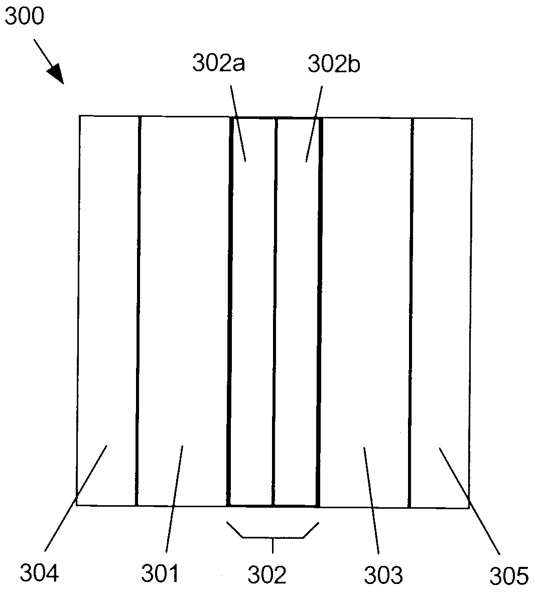
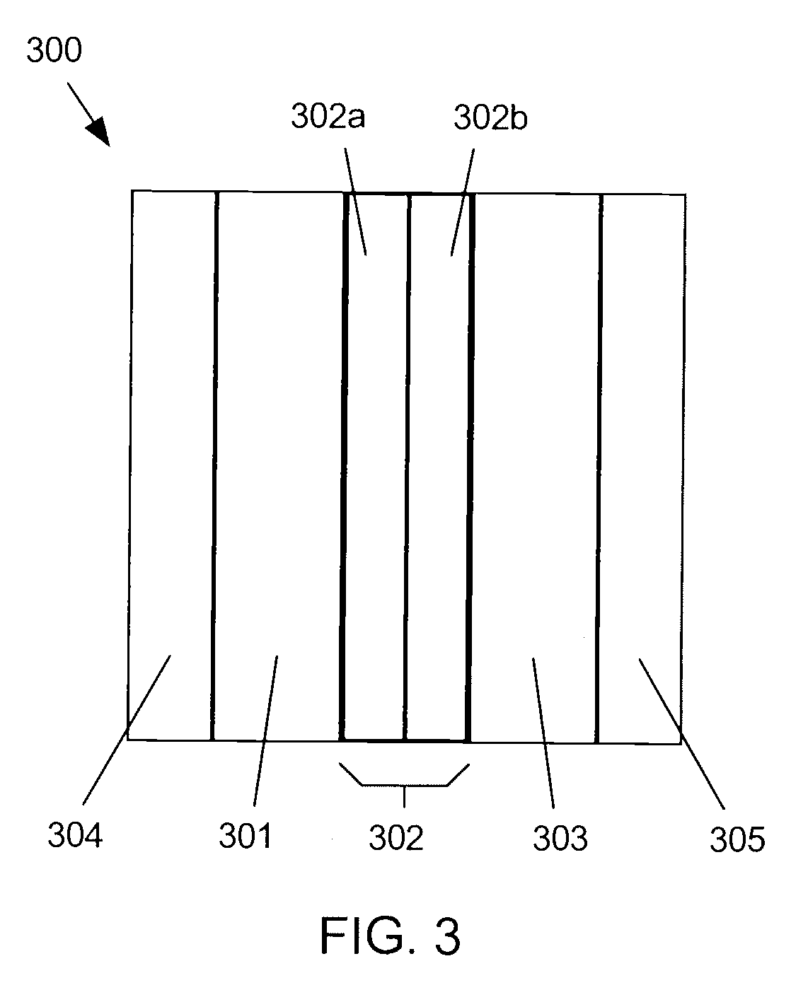
[0013]FIG. 3 shows an electrochromic device 300 according to the present invention. Electrochromic device 300 includes an EC layer 301, an IC layer 302 and a CE layer 303, which may also be electrochromic. Layers 301-303 are positioned between two TCO layers 304 and 305. IC layer 302 is a bilayer ion conductor (IC) layer 302 having first IC layer 302a and second IC...


PUM


Abstract

An electrochromic device includes a first conductive layer, a dual-layer ion conductor layer, and a second conductive layer. The first ion conductor layer and the second ion conductor layer are formed from different materials and/or by different processes. The layers are deposited using PVD, CVD, or plating techniques.

Description

[0001]This application claims the benefit of U.S. Provisional Patent Application Ser. No. 60 / 933,869 filed Jun. 7, 2007.BACKGROUND OF THE INVENTION[0002]1. Field of Invention[0003]The present invention relates to electrochromic devices, and more particularly to electrochromic devices having dual-layer ion conductors and methods for making such ion conductors.[0004]2. Description of the Prior Art[0005]Electrochromic materials are materials that change their optical properties as the result of an applied electrical potential. Such materials can be used to produce electrochromic devices that can vary the transmission or reflectance of electromagnetic radiation via application of an electrical potential. FIGS. 1 and 2 depict a typical prior art electrochromic device 100. Electrochromic device 100 includes an electrochromic (EC) layer 101, an ion conductor (IC) layer 102 and a counter-electrode (CE) layer 103, which may also be electrochromic. Layers 101-103 are positioned between two tr...

Claims


Application Information

Patent Timeline
IPC IPC(8): G02F1/15
CPCG02F1/1525
Inventor NGUYEN, PAUL
Owner VIEW INC
Why Eureka
Try Eureka