Semiconductor device

Inactive Publication Date: 2009-04-16
RENESAS ELECTRONICS CORP
View PDF9 Cites 4 Cited by
  • Summary
  • Abstract
  • Description
  • Claims
  • Application Information

AI Technical Summary

Benefits of technology

[0013]According to the present invention, it is therefore possible to provide a technique that can prevent the separa

Problems solved by technology

Consequently, the difference between the linear expansion rates of the island and the sealing resin is reduced, thereby the island and the sealing resin are not separated so easily.
Thus the silicon and the copper material are also not separated so easily.
As a resu

Method used


Image

  • Semiconductor device
  • Semiconductor device
  • Semiconductor device

Examples


Example

[0020]Hereunder, the embodiments of the present invention will be described with reference to the accompanying drawings. In all of those drawings, same reference numerals will be used for same components, avoiding redundant description.

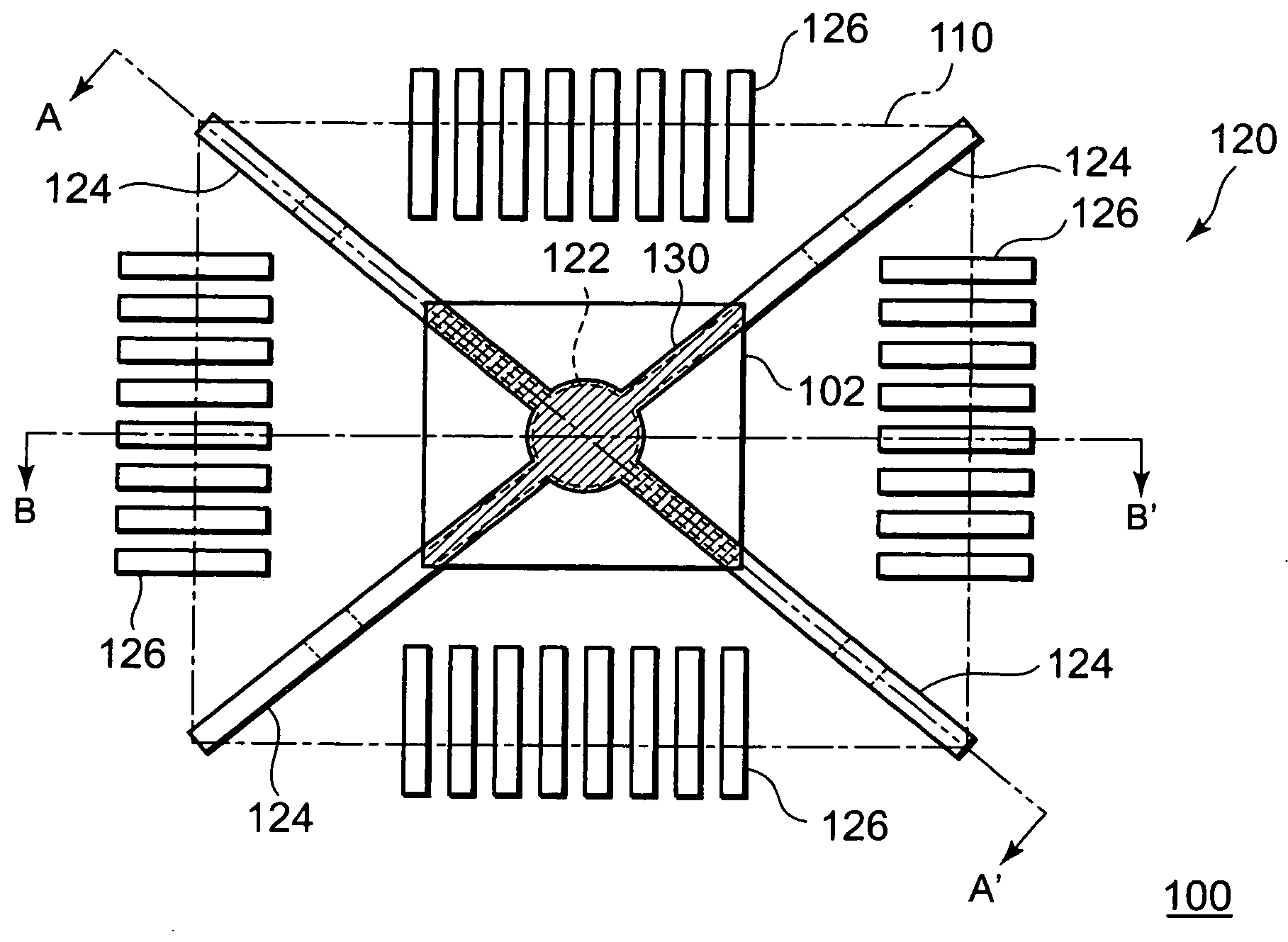
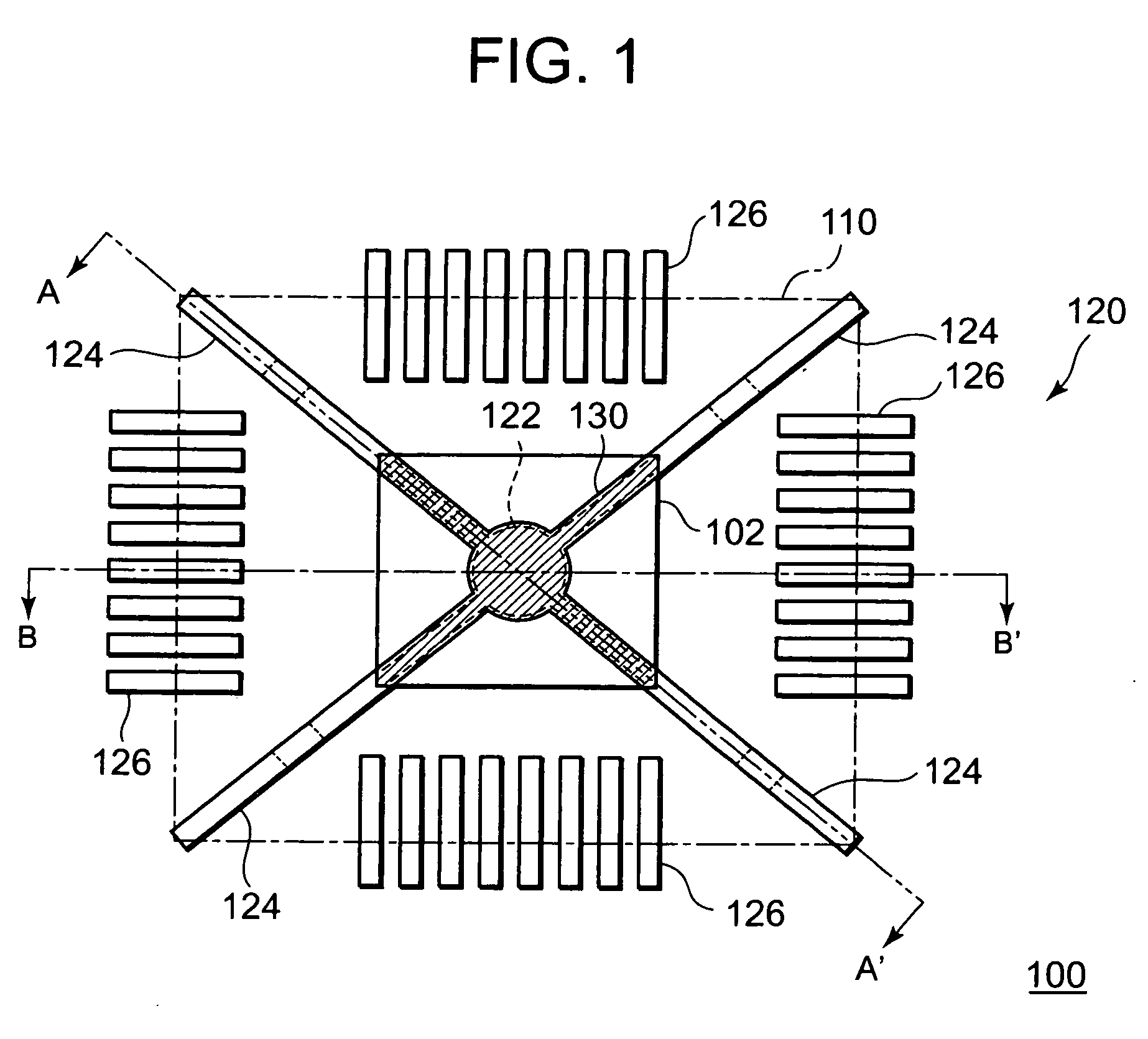
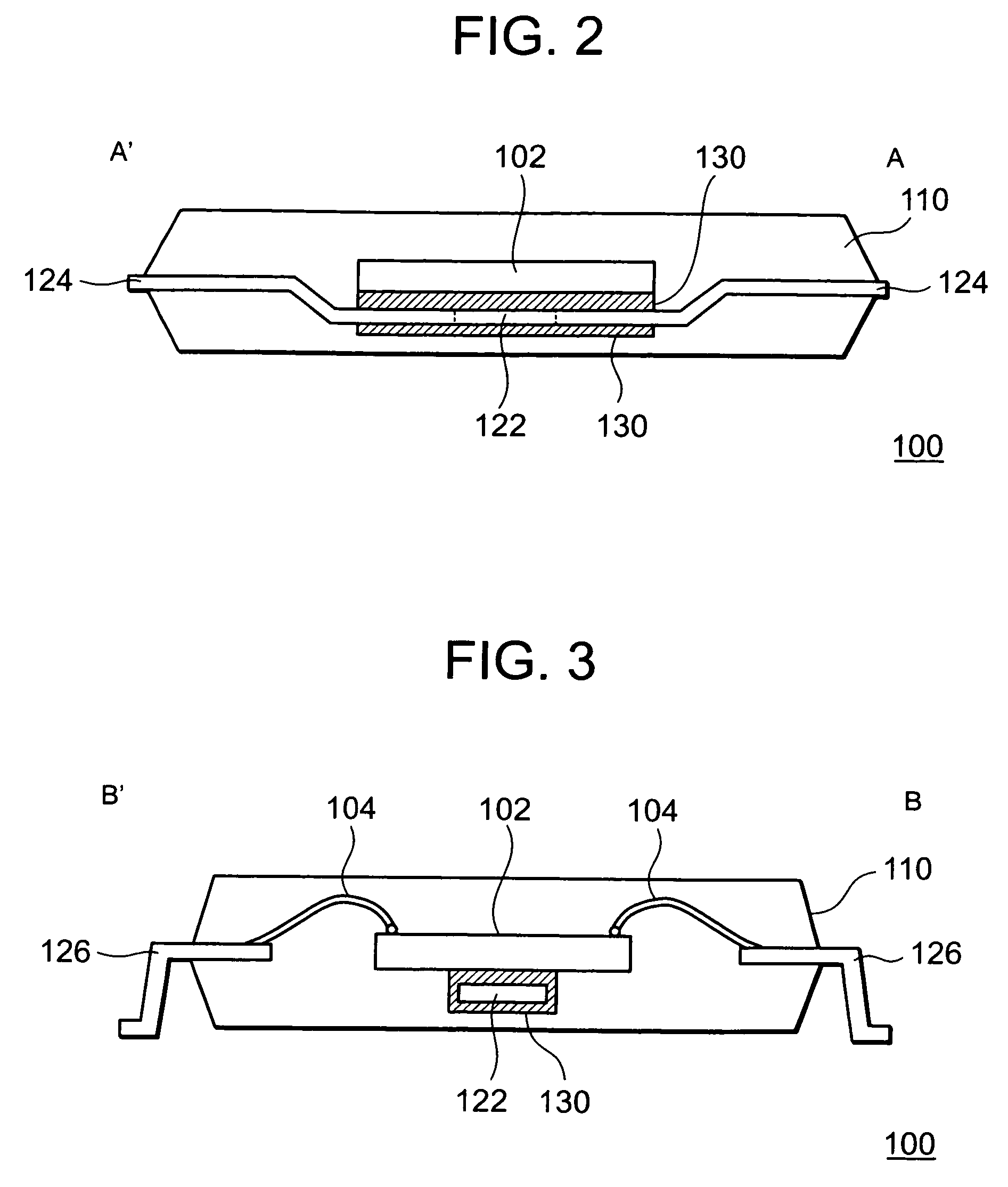
[0021]FIG. 1 shows a bottom view of a configuration of a semiconductor device in an embodiment of the present invention. FIG. 2 shows a cross sectional view taken on line A-A′ of FIG. 1. FIG. 3 shows a cross sectional view taken on line B-B′ of FIG. 1. The bottom view shown in FIG. 1 is taken from the lower side in FIGS. 2 and 3.

[0022]The semiconductor device 100 includes a semiconductor chip 102; a lead device 120 consisting of an island 122 for mounting the semiconductor chip 102, plural hanging leads 124, and plural external leads 126; a mounting material 130 provided on a contact surface between each of the island 122 and hanging leads 124 and the semiconductor chip 102 and used to adhere the semiconductor chip 102 to the island 122 and the hangin...


PUM


Abstract

Disclosed herewith is a semiconductor device, which includes a semiconductor chip; a lead device that includes an island for mounting the semiconductor chip and having an area smaller than that of the semiconductor chip at its contact surface, as well as plural hanging leads for supporting the island and coming in contact partially with the semiconductor chip; a mounting material provided on a contact surface between each of the island and hanging leads and the semiconductor chip so as to adhere the semiconductor chip to the island and the hanging leads; and sealing resin for sealing the semiconductor chip. The modulus of elasticity of the mounting material is lower than that of the sealing resin. The mounting material is further coated on the back surfaces of the contact surfaces of the island and the hanging leads.

Description

FIELD OF THE INVENTION[0001]The present invention relates to a semiconductor device.BACKGROUND OF THE INVENTION[0002]The patent document 1 (JP-A-HEI03-022465) discloses a resin sealing type semiconductor device having a semiconductor element (chip) sealed with resin. In the configuration of this semiconductor device, the semiconductor element is mounted on an island larger in size than the semiconductor element. In this case, both the front surface of the semiconductor element and the back surface of each lead frame disposed on the island are coated with a polyimide-based resin film having a thickness of 5 to 100 μm so as to give favorable adherence to both the sealing resin and the semiconductor element / lead frames and absorb the stress to be generated between the sealing resin and each of the semiconductor element / lead frames.[0003]However, if the surface of the semiconductor element is also coated with a polyimide-based resin film in such a way according to the technique as discl...

Claims


Application Information

Patent Timeline
IPC IPC(8): H01L23/495
CPCH01L23/49503H01L23/49513H01L2924/01033H01L2924/01006H01L24/48H01L24/32H01L2924/01082H01L2924/01029H01L2224/32014H01L2224/32245H01L2224/48091H01L2224/48247H01L2224/73265H01L2924/01005H01L2924/01027H01L2924/00014H01L2924/3512H01L2924/00H01L2924/181H01L2924/00012H01L2224/45099H01L2224/45015H01L2924/207
Inventor KIMURA, NAOTO
Owner RENESAS ELECTRONICS CORP
Why Eureka
Try Eureka