Image forming apparatus

a technology of image forming apparatus and forming apparatus, which is applied in the direction of electrographic process apparatus, instruments, optics, etc., can solve the problems of reducing the transfer rate and density of toner in resulting images, and weak transfer field to attract toner particles

Inactive Publication Date: 2009-08-06
RICOH KK
View PDF3 Cites 31 Cited by
  • Summary
  • Abstract
  • Description
  • Claims
  • Application Information

AI Technical Summary

Benefits of technology

[0014]Exemplary aspects of the present invention are put forward in view of the above-described circumstances, and provide a novel image forming apparatus that can optimize a transfer bias used to transfer a toner image across a transfer gap.

Problems solved by technology

For example, with too low a bias voltage applied to the biasing member, the resulting transfer field is too weak to attract toner particles.
On the other hand, too high a bias voltage makes too strong a transfer field that induces an electrical discharge in the transfer nip.
In either case, an inappropriate transfer field reduces transfer rate and density of toner in resulting images.
In particular, the electrical discharge in the transfer nip is known to disturb transfer of toner, and can cause “reverse transfer”, in which toner that has been transferred from an upstream photoconductor retransfers to a downstream photoconductor during sequential transfer of toner to a single receiving surface.
However, such optimization is difficult to achieve since the transfer bias is sensitive to variations in operating conditions, such as temperature and humidity, resistance of recording sheets, charge amounts of toner, and settings of specific print jobs.
Designed to stabilize transfer rate at relatively low transfer bias voltages, these conventional methods do not account for effects of an excessive transfer bias on transfer performance, and therefore, cannot prevent image degradation due to an electric discharge occurring in the transfer gap.
Unfortunately, these detection techniques are designed for use in developing devices, and cannot be applied to the detection of an electrical discharge during transfer of developed toner images.

Method used


Image

  • Image forming apparatus
  • Image forming apparatus
  • Image forming apparatus

Examples


experiment 1

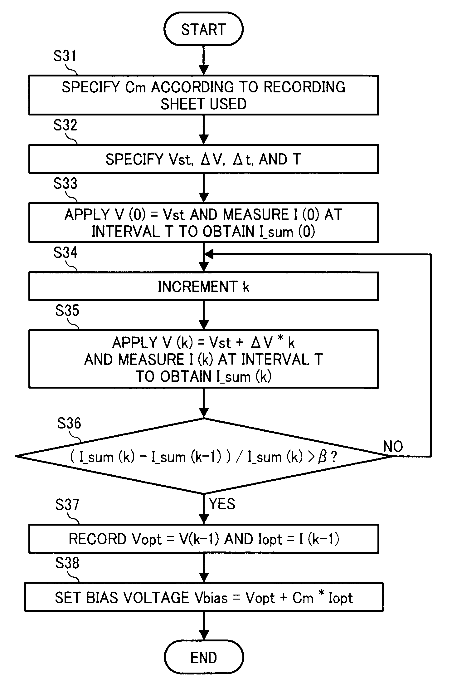
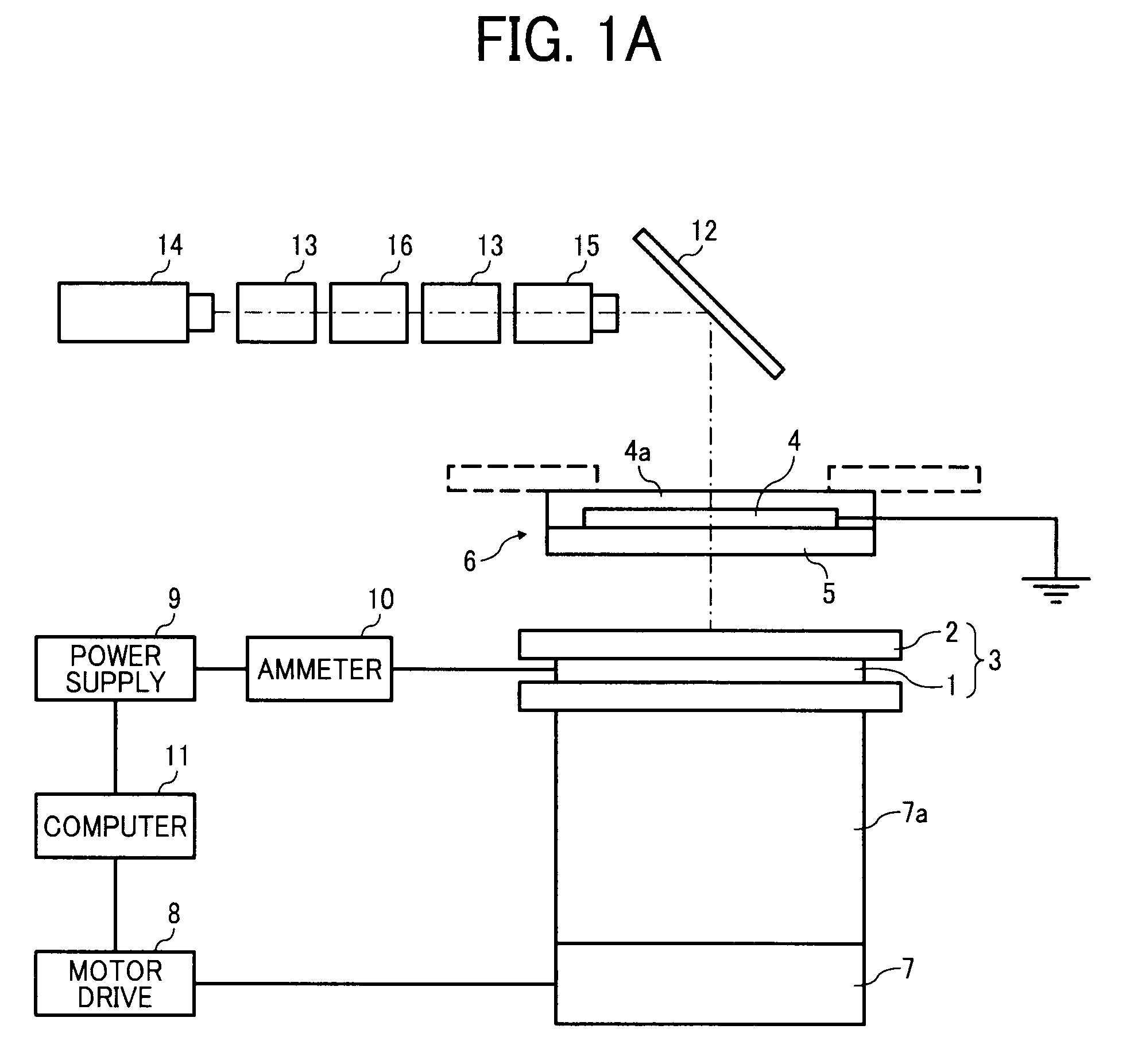
[0046]The ITO substrate 6 bearing a developed toner image thereon was set in place, and the stepper motor 7 moved the SS-PI substrate 3 closer to the ITO substrate 6 while the power supply 9 applied a given constant voltage to the SS electrode 1 so as to transfer toner particles from the PC surface to the PI surface. After transfer, the lower substrate 3 was retracted away from the upper substrate 6, and the weight of toner particles present on the PI sheet 2 was measured.

[0047]The above procedure was repeated using different bias voltages ranging from 0 to 1700 V, for each of which a transfer rate of toner was calculated according to the following equation:

Transfer rate(%)=Wa / Wb*100   Equation 1

where “Wa” is an amount of toner particles present on the PI surface after transfer, and “Wb” is an amount of toner particles forming an image developed on the PC-ITO substrate prior to transfer.

[0048]FIG. 2 shows results of Experiment 1, plotting calculated transfer rates against applied tr...

experiment 2

[0051]The ITO substrate 6 bearing a developed toner image thereon was set in place, and the stepper motor 7 moved the SS-PI substrate 3 closer to the ITO substrate 6 while the power supply 9 applied a stepped-up voltage to the SS electrode 1 so as to transfer toner particles from the PC surface to the PI surface. During transfer, the ammeter 10 measured the current flowing into the SS electrode 1 with the bias voltage increased from 170 V to 1700 V in steps of 170 V per millisecond.

[0052]FIG. 3 shows measurement results of Experiment 2, plotting the output current in microamperes (solid line) with the applied bias voltage in volts (dotted line) against time in milliseconds.

[0053]As shown in FIG. 3, the current output to the electrode 1 traces a substantially regular, periodic waveform when the bias voltage is stepped up to 1190 V, except for the first millisecond in which the current level still remains low. The output current significantly increases as the applied voltage increases...

experiment 3

[0109]Printing was performed using plain A4 size copy paper (T6200 A4Y available from Ricoh Company Ltd.) and a direct transfer tandem color printer.

[0110]Initially, development was performed with suitable photoconductor charge and development bias so as to obtain a monochrome solid image with an area of 8 cm2 and a toner density of 0.4 mg / cm2 on the photoconductor drum. The toner image was then transferred to the copy paper by applying a given current bias. After transfer, the print engine was halted, and toner particles remaining on the surface of the photoconductor were collected by suction.

[0111]The above procedure was repeated with various transfer bias currents (5, 10, 20, 30, 40, 50, and 60 μA), for each of which a transfer rate was calculated according to the following equation:

Transfer rate(%)=(Wc−Wd) / Wc*100   Equation 3

[0112]where “Wc” is the weight of toner present on the photoconductor prior to transfer, and “Wd” is the weight of toner remaining on the photoconductor aft...


PUM


Abstract

An image forming apparatus includes a transfer device, a voltage applicator, a current sensor, and a discharge detector. The transfer device transfers a toner image from one surface to another by developing an electrical field across a transfer gap when provided with a transfer bias. The voltage applicator applies a stepped test voltage to the transfer device. The current sensor senses a current flowing to the transfer device during application of the test voltage the discharge detector detects an electrical discharge occurring in the transfer gap based on a rate of increase of the sensed current.

Description

CROSS-REFERENCE TO RELATED APPLICATIONS[0001]The present patent application claims priority pursuant to 35 U.S.C. §119 from Japanese Patent Application No. 2008-026923 filed on Feb. 6, 2008, the contents of which are hereby incorporated by reference herein in their entirety.BACKGROUND OF THE INVENTION[0002]1. Field of the Invention[0003]The present invention relates to an electrophotographic image forming apparatus, and more particularly, to an image forming apparatus incorporating a transfer bias optimizer that optimizes an electrical transfer bias used to transfer a toner image in electrophotographic imaging processes.[0004]2. Discussion of the Background[0005]In electrophotography, images developed with toner particles are transferred from one medium to another during several imaging processes. Many electrophotographic image forming apparatuses employ transfer devices to transfer toner images across a transfer nip or gap, in which a biasing member, such as a roller, brush, or cor...

Claims


Application Information

Patent Timeline
Patent Type & Authority Applications(United States)
IPC IPC(8): G03G15/00G03G15/16
CPCG03G15/0131G03G2215/0129G03G15/1605
Inventor SUKESAKO, MASAKIKOINUMA, NOBUYUKISUDO, KAZUHISAYUKI, KAZUHIKOTAKAHASHI, HIROAKIMIZUTANI, TAKEHIDEYOSHIDA, RYUJI
Owner RICOH KK
Why Eureka
Try Eureka