Nonvolatile semiconductor memory device

Inactive Publication Date: 2009-10-08
HITACHI LTD
View PDF4 Cites 1 Cited by
  • Summary
  • Abstract
  • Description
  • Claims
  • Application Information

AI Technical Summary

Benefits of technology

[0019]Next, the potential of the selected word line SWL is increased from 0 V to about 20 V. At this time, in bit lines BL2n−2 and BL2n in which the potential of the surface of the substrate is at 0 V, a large potential difference occurs between the floating gate and the surface of the substrate, so that electron is injected from the surface of the substrate to the floating gate by the tunnel current, thereby causing the programming. On the other hand, in bit lines BL2n−1 and BL2n+1 in which the potential of the surface of the substrate is at VH, the potential difference between the floating gate and the surface of the substrate is relaxed, thereby not causing the programming.
[0029]Accordingly, one object of the present invention is to provide a technique in which a reduction of the programming-prevent voltage is suppressed so that the miss-programming to the unselected memory cell is prevented in the nonvolatile semiconductor memory device.
[0035](1) It can suppress a word disturbance which increases as a width of a shallow isolation trench is narrower by scaling down of a pitch of a bit line.
[0036](2) It can improve reliability of a nonvolatile semiconductor memory device.

Problems solved by technology

For example, a defect by the capacitive coupling with the reduction of memory cell size of the NAND-type flash memory occurs not only between the floating gates.
This becomes a cause to reduce the reliability of the NAND-type flash memory as well as the above-described threshold voltage shift by the capacitive coupling between the floating gates.

Method used


Image

  • Nonvolatile semiconductor memory device
  • Nonvolatile semiconductor memory device
  • Nonvolatile semiconductor memory device

Examples


first embodiment

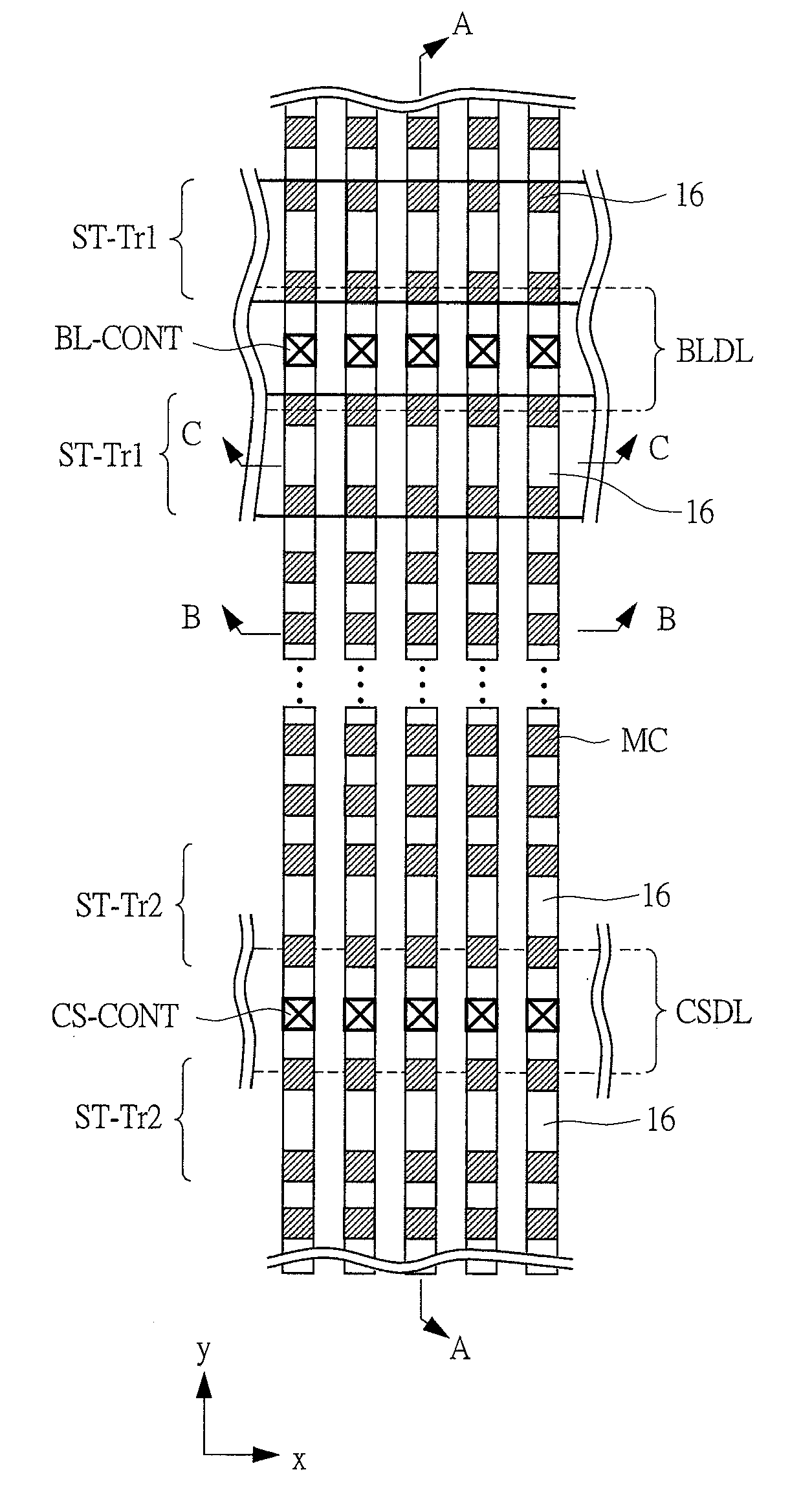
[0064]FIG. 11 is a diagram showing a part of configuration of a memory cell array in a nonvolatile semiconductor memory device according to a first embodiment of the present invention, and shows an example of a voltage condition in the programming to A page.

[0065]A nonvolatile semiconductor memory device according to a first embodiment of the present invention is a nonvolatile semiconductor memory device which is electrically capable of programming / erasing, and for example, it is a NAND-type flash memory which is capable of bulk erasing. The nonvolatile semiconductor memory device according to the first embodiment is formed by a general configuration including, for example, a memory cell array, a decoder, a sense latch circuit, data latch circuit, a main amplifier, an input data arithmetic circuit, an input / output buffer, a control signal input buffer, a data input / output control circuit, a ready / busy circuit, a system clock circuit, a command decoder, and others. And, the nonvolati...

second embodiment

[0078]While the programming is performed in dividing the cell under the selected word line SWL into 3 pages in the first embodiment, the programming can be also performed in dividing the cell under the selected word line SWL into 4 or more pages.

[0079]FIG. 14 is an example showing a voltage condition in a programming in a nonvolatile semiconductor memory device according to a second embodiment of the present invention.

[0080]As shown in FIG. 14, groups are made so as to divide the bit line BL into each 3 bit lines, and each of the groups is an A page, a B page, a C page, and a D page. And, a voltage (for example, 20 V) is applied to the selected word line SWL, and the bit line voltage (for example, 3 V) is applied so as to programming-prevent in all of B, C, and D pages when the programming is performed to A page. In such a manner, the programming-prevent voltage VH is surely provided on at least one side of both surfaces of the semiconductor substrate which are adjacent via the shal...

third embodiment

[0082]In a third embodiment, such an operation is performed that, the programming to A, B, and C pages are gradually performed when the programming is performed in dividing the cell under the selected word line SWL into the 3 pages in the first embodiment and then the programming is ended at a stage that threshold voltages of all of memory cells in all of A, B, and C pages eventually reach a target threshold voltage.

[0083]FIG. 15 is a flow chart showing a programming sequence in a nonvolatile semiconductor memory device according to a third embodiment of the present invention.

[0084]The programming in the nonvolatile semiconductor memory device according to the third embodiment of the present invention is executed by the following sequence.

[0085]First, the programming is performed to A page (BL3n+1) in a step S101. Next, the programming is performed to B page (BL3n+2) in a step S102. Next, the programming is performed to C page (BL3n+3) in a step S103.

[0086]Next, in a step S104, the ...


PUM


Abstract

A nonvolatile semiconductor memory device according to the present invention is a NAND-type flash memory which is electrically capable of programming / erasing. The nonvolatile semiconductor memory device has at least 3 or more memory cell columns in which a plurality of memory cells are connected in series, and these memory cell columns are adjacent to each other via a shallow trench isolation. And, a programming operation is performed individually to each of these memory cell columns. In this manner, a programming-prevent voltage is surely provided at on at least one side of both surfaces of the semiconductor substrate which are adjacent via a shallow trench isolation to the surface of the semiconductor substrate under the programming-prevented memory cell. Therefore, a miss-programming to an unselected memory cell can be largely reduced.

Description

CROSS-REFERENCE TO RELATED APPLICATION[0001]The present application claims priority from Japanese Patent Application No. 2008-99104 filed on Apr. 7, 2008, the content of which is hereby incorporated by reference into this application.TECHNICAL FIELD OF THE INVENTION[0002]The present invention relates to a nonvolatile semiconductor memory device. More particularly, the present invention relates to a technique to realize high integration and high performance of a nonvolatile semiconductor memory device which is electrically capable of programming / erasing.BACKGROUND OF THE INVENTION[0003]As a technique which the inventors have studied, for example, the following techniques are considered in a nonvolatile semiconductor memory device.[0004]Among nonvolatile semiconductor memory devices which are electrically capable of programming / erasing, so-called flash memory is known as the one which is capable of bulk erasing. Since the flash memory is excellent in portability and impact resistance ...

Claims


Application Information

Patent Timeline
IPC IPC(8): G11C16/02G11C16/06
CPCG11C16/0483G11C16/3427G11C16/3418G11C16/10
InventorSASAGO, YOSHITAKAKUME, HITOSHI
OwnerHITACHI LTD