Buried asymmetric junction ESD protection device

a protection device and asymmetric junction technology, applied in the direction of semiconductor devices, semiconductor/solid-state device details, electrical apparatus, etc., can solve the problems of increasing the overall manufacturing cost, reducing the overall manufacturing yield, and difficult or impossible to achiev

Inactive Publication Date: 2010-01-28
NXP USA INC
View PDF4 Cites 9 Cited by
  • Summary
  • Abstract
  • Description
  • Claims
  • Application Information

AI Technical Summary

Problems solved by technology

One of the difficulties of using bipolar transistors for ESD devices is that their turn-on voltages Vt1 for DC operation (i.e., Vt1DC) and transient operation (i.e., Vt1TR) are often different, i.e., Vt1DC is not equal to Vt1TR.
However

Method used


Image

  • Buried asymmetric junction ESD protection device
  • Buried asymmetric junction ESD protection device
  • Buried asymmetric junction ESD protection device

Examples


first embodiment

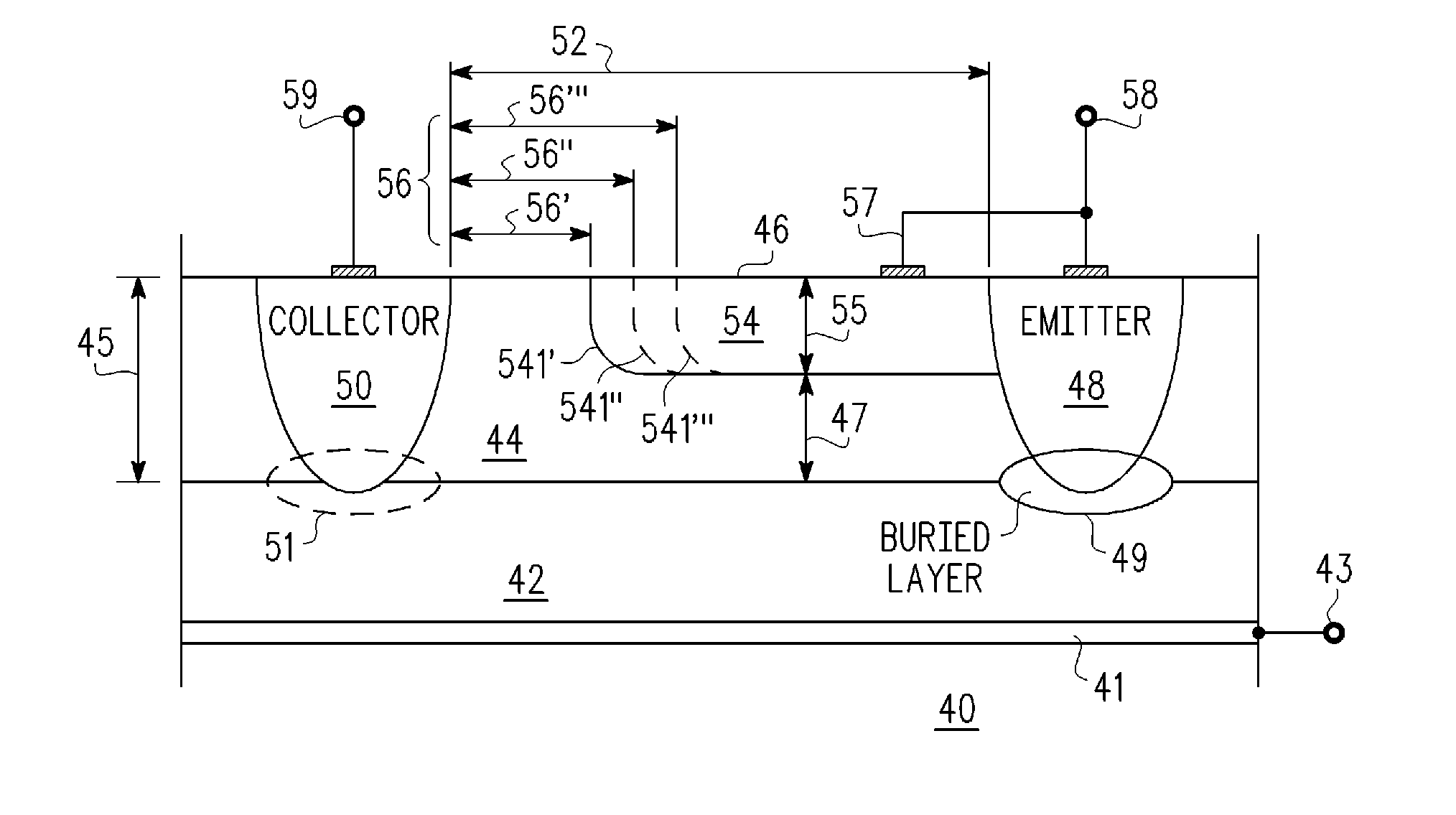
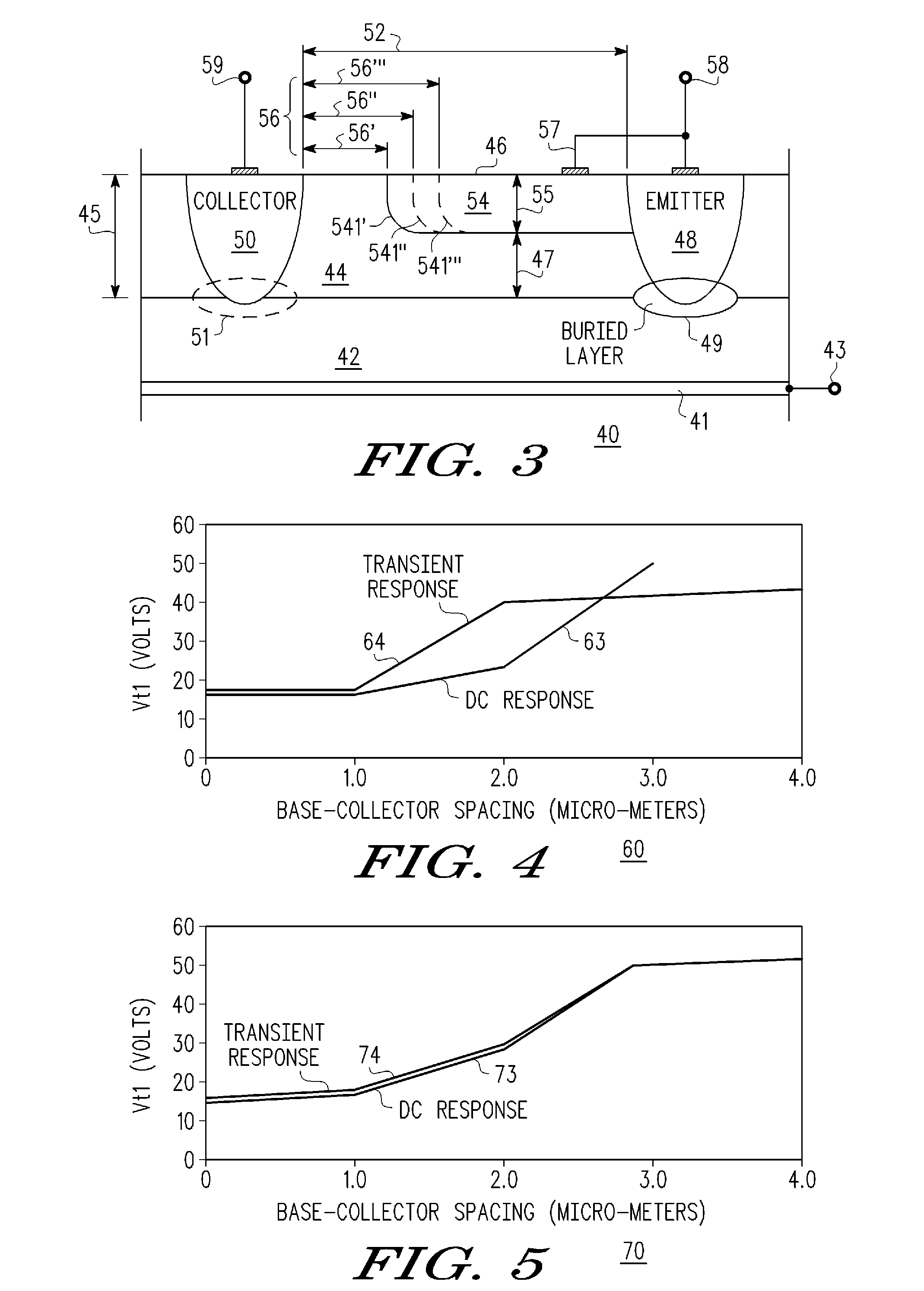
[0020] there is provided a lateral electrostatic discharge (ESD) protection device (40), comprising, a semiconductor substrate (42) of a first conductivity type and first doping level, a semiconductor layer (44) overlying the substrate (42), and of the first conductivity type and a second doping level and having an outer surface (46) spaced a first distance (45) from the substrate (42), emitter (48) and collector (50) regions of a second, opposite, conductivity type, laterally spaced apart by a second distance (52), and having third doping level greater than the second doping level, a well region (54) of the first conductivity type in but not extending through the semiconductor layer (44) and having a doping level higher than the second doping level but less than or equal to the third doping level, and extending laterally from the emitter region (48) toward but separated from the collector region (50) by a third distance (56), and a buried layer (49) of the second conductivity type ...

second embodiment

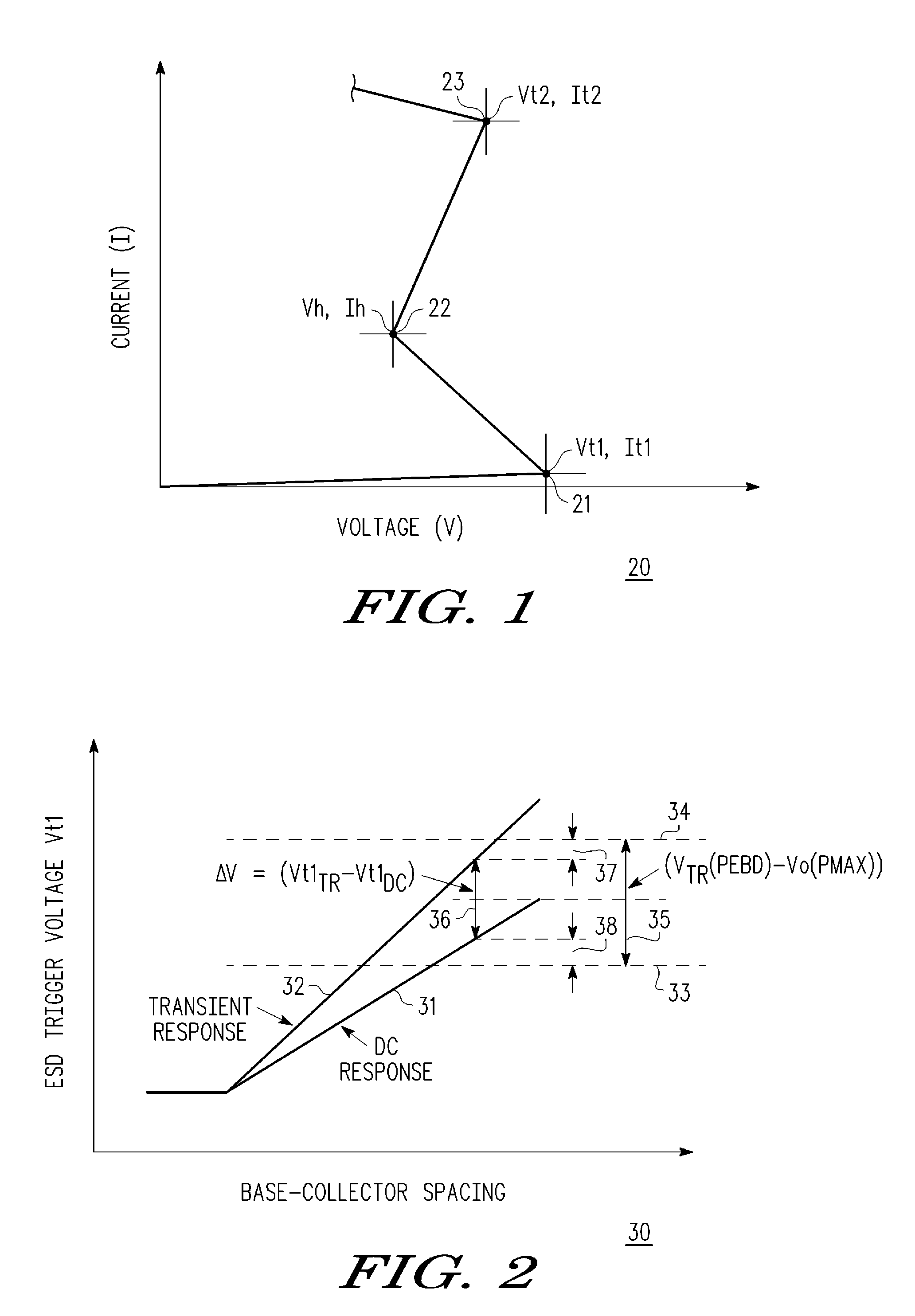
[0021] there is provided a lateral bipolar electrostatic discharge (ESD) protection device (40) having a trigger voltage Vt1, comprising, a semiconductor (SC) substrate (42), an overlying epitaxial SC layer (44), emitter-collector regions (48, 50) in the SC layer (44), laterally spaced apart by a first distance (52), a base region (54) adjacent the emitter region (48) in the epitaxial SC layer (44) extending laterally toward and separated from the collector region (50) by a base-collector spacing (56) in the epitaxial layer (44), which base-collector spacing (56) is chosen to set a predetermined ESD trigger voltage Vt1, and a buried layer region (49) under the emitter region (48) Ohmically coupled thereto, but without a comparable buried layer region (51) under the collector region (50), thereby providing an asymmetrical structure whose DC trigger voltage (Vt1DC) and transient trigger voltage (Vt1TR) are approximately equal. According to a further embodiment, the buried layer region...

third embodiment

[0022] there is provided a lateral electrostatic discharge (ESD) protection device (40), comprising, a semiconductor substrate (42) of a first conductivity type and first doping level, a semiconductor layer (44) overlying the substrate (42), and of the first conductivity type and a second doping level equal or less than the first doping level and having an outer surface (46) spaced a first distance (45) from the substrate (42), emitter (48) and collector (50) regions of a second, opposite, conductivity type, laterally spaced apart by a second distance (52), and having third doping levels greater than the second doping level, a well region (54) of the first conductivity type in but not extending through the semiconductor layer (44) and having a doping level higher than the second doping level and extending laterally from the emitter region (48) toward but separated from the collector region (50) by a third distance (56), wherein the third distance (56) is in the range of about 0 to 3...


PUM


Abstract

An improved lateral bipolar electrostatic discharge (ESD) protection device (40) comprises a semiconductor (SC) substrate (42), an overlying epitaxial SC layer (44), emitter-collector regions (48, 50) laterally spaced apart by a first distance (52) in the SC layer, a base region (54) adjacent the emitter region (48) extending laterally toward and separated from the collector region (50) by a base-collector spacing (56) that is selected to set the desired trigger voltage Vt1. By providing a buried layer region (49) under the emitter region (48) Ohmically coupled thereto, but not providing a comparable buried layer region (51) under the collector region (50), an asymmetrical structure is obtained in which the DC trigger voltage (Vt1DC) and transient trigger voltage (Vt1TR) are closely matched so that ∥Vt1TR−Vt1DC∥˜0. This close matching increases the design margin and provides a higher performance ESD device (40) that is less sensitive to process variations, thereby improving manufacturing yield and reducing cost.

Description

FIELD OF THE INVENTION[0001]The present invention generally relates to semiconductor (SC) devices and integrated circuits (ICs) and, more particularly, structures and methods for forming electrostatic discharge (ESD) protection devices for ICs and other SC and non-SC devices.BACKGROUND OF THE INVENTION[0002]FIG. 1 shows simplified plot 20 of transmission line pulse current (I) versus voltage (V) for a typical electrostatic discharge (ESD) protection device. As the applied voltage is increased, very little current flows until triggering voltage 21 is reached at voltage Vt1. Once triggered into operation, the ESD device conducts and the current increases to holding point 22 with current Ih and voltage Vh. Depending upon the internal impedance of the voltage source, current and voltage may further increase to point 23 at current It2 and voltage Vt2, beyond which destructive failure may occur leading to further current increase accompanied by voltage decrease. Electrostatic discharge (E...

Claims


Application Information

Patent Timeline
IPC IPC(8): H01L23/62
CPCH01L29/735H01L29/861H01L27/0259
Inventor GILL, CHAI EANHONG, CHANGSOOWHITFIELD, JAMES D.ZHAN, ROUYING
Owner NXP USA INC
Why Eureka
Try Eureka