Method of Manufacturing a Light Emitting, Photovoltaic or Other Electronic Apparatus and System

a technology of photovoltaic or other electronic equipment and system, applied in the field of light emitting and photovoltaic technology, can solve the problems of difficulty in generating widespread use, difficulty in reducing the cost of finished products, and insufficient energy saving

Active Publication Date: 2010-03-18
NTHDEGREE TECH WORLDWIDE +1
View PDF100 Cites 62 Cited by
  • Summary
  • Abstract
  • Description
  • Claims
  • Application Information

AI Technical Summary

Benefits of technology

[0014]The exemplary embodiments of the present invention provide a new type of LED-based lighting devices and photovoltaic devices, and new methods of manufacturing such devices, using printing and coating technologies. The inventive photovoltaic and/or LED-based lighting devices may be fabricated in a wide variety of sizes, from a size comparable to a mobile telephone display, to that of a billboard display (or larger). The exemplary inventive photovoltaic and/or LED-based lighting devices are also robust and capable of operating under a wide variety of conditions, including outdoor and other stressful environmental conditions. The exemplary inventive methods of manufacturing photovoltaic and/or LED-based lighting devices utilize comparatively low temp

Problems solved by technology

This is a time consuming, labor intensive and expensive process, resulting in LED-based lighting devices which are generally too expensive for many consumer applications.
This is also a time consuming, labor intensive and expensive process, resulting in photovoltaic devices which are also too expensive for widespread use without being subsidized or without other governmental incentives.
U.S. Pat. No. 6,706,959, issued Mar. 16, 2004 and entitled “Photovoltaic Apparatus and Mass Producing Apparatus for Mass Producing Spherical Semiconducting Particles” disclose a method which initially uses spherical diodes having a pn junction formed about the entire sphere, but then introduce manufacturing problems by requiring corresponding micromachining of each individual diode to remove a substantial section of the sphere and its pn junction, to form a recess into an inner, core portion.
Again, this is also a time consuming, labor intensive and expensive process, with corresponding difficulties for generating widespread use.
This micromachining method did not gain wide acceptance, possibly due to many difficulties which we

Method used


Image

  • Method of Manufacturing a Light Emitting, Photovoltaic or Other Electronic Apparatus and System
  • Method of Manufacturing a Light Emitting, Photovoltaic or Other Electronic Apparatus and System
  • Method of Manufacturing a Light Emitting, Photovoltaic or Other Electronic Apparatus and System

Examples


Embodiment Construction

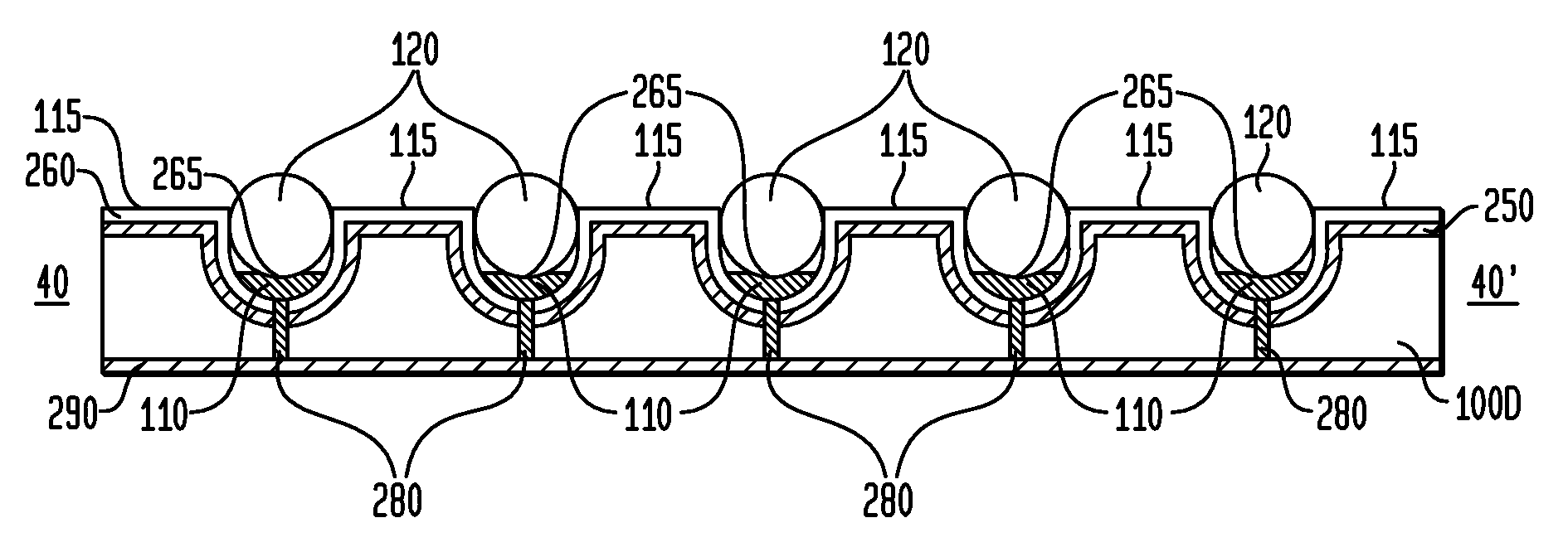
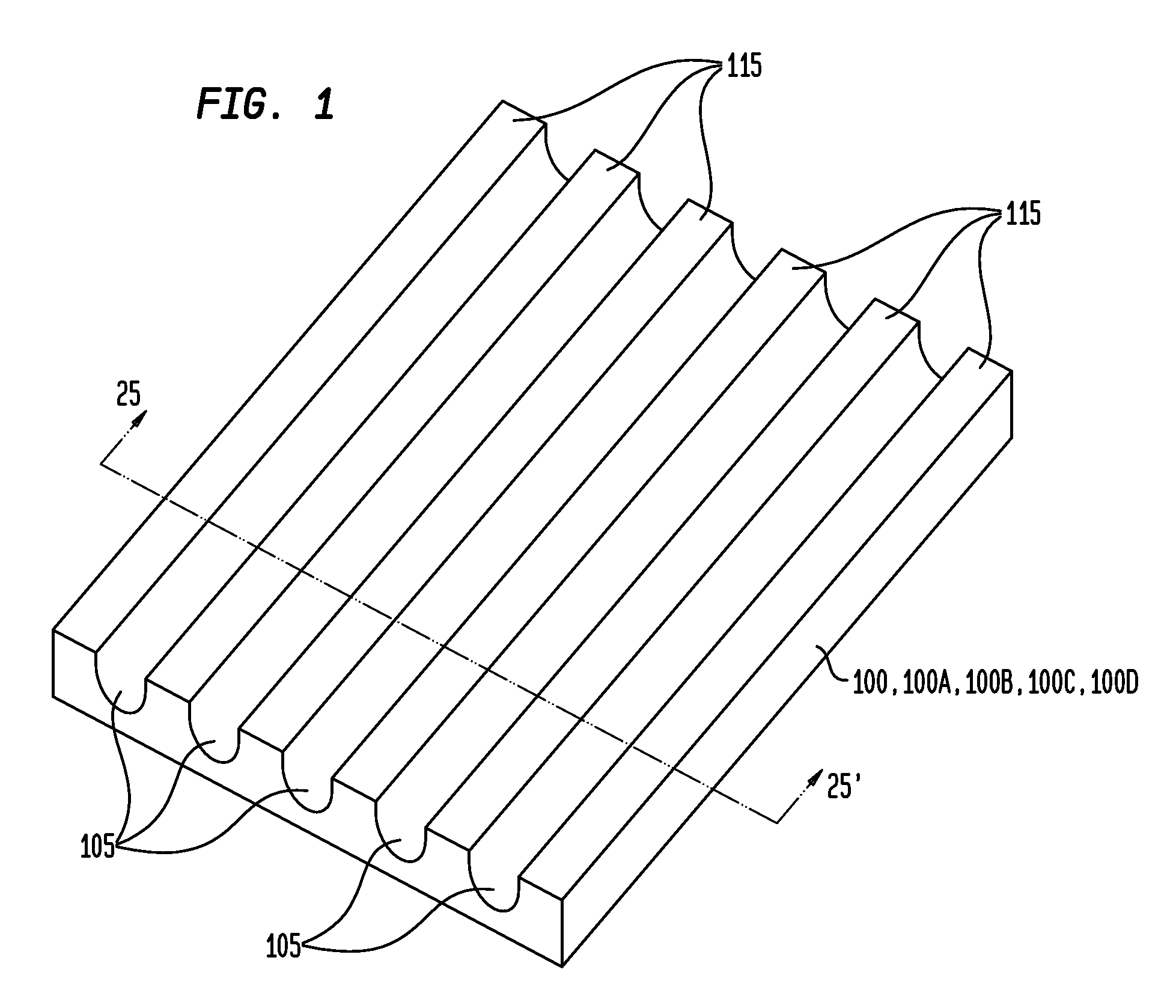
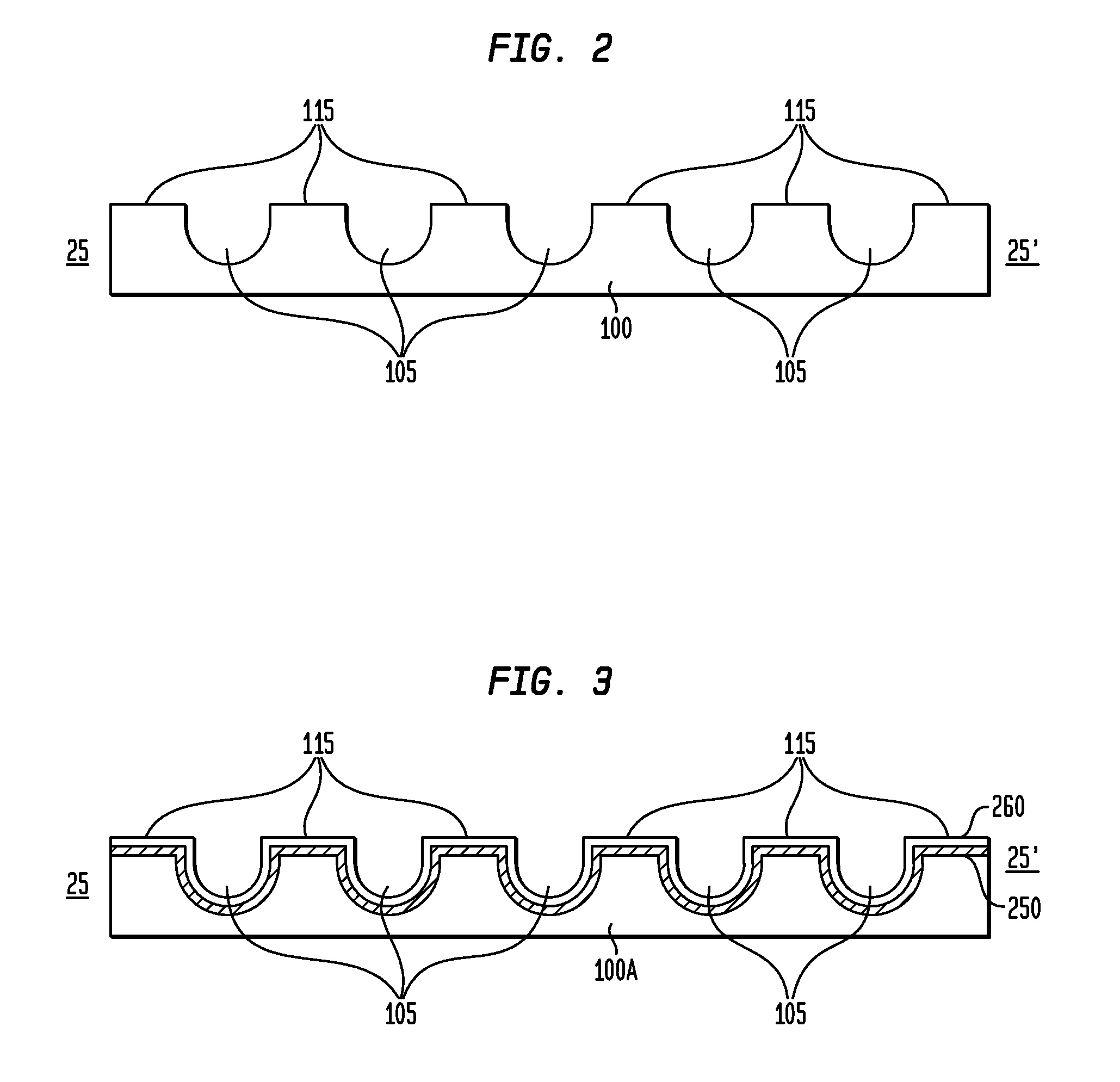
[0104]While the present invention is susceptible of embodiment in many different forms, there are shown in the drawings and will be described herein in detail specific exemplary embodiments thereof, with the understanding that the present disclosure is to be considered as an exemplification of the principles of the invention and is not intended to limit the invention to the specific embodiments illustrated. In this respect, before explaining at least one embodiment consistent with the present invention in detail, it is to be understood that the invention is not limited in its application to the details of construction and to the arrangements of components set forth above and below, illustrated in the drawings, or as described in the examples. Methods and apparatuses consistent with the present invention are capable of other embodiments and of being practiced and carried out in various ways. Also, it is to be understood that the phraseology and terminology employed herein, as well as...


PUM


Abstract

The present invention provides a method of manufacturing an electronic apparatus, such as a lighting device having light emitting diodes (LEDs) or a power generating device having photovoltaic diodes. The exemplary method includes forming at least one first conductor coupled to a base; coupling a plurality of substantially spherical substrate particles to the at least one first conductor; converting the substrate particles into a plurality of substantially spherical diodes; forming at least one second conductor coupled to the substantially spherical diodes; and depositing or attaching a plurality of substantially spherical lenses suspended in a first polymer. The lenses and the suspending polymer have different indices of refraction. In some embodiments, the lenses and diodes have a ratio of mean diameters or lengths between about 10:1 and 2:1. In various embodiments, the forming, coupling and converting steps are performed by or through a printing process.

Description

CROSS-REFERENCE TO RELATED APPLICATIONS[0001]This application is a continuation-in-part of and claims priority to U.S. patent application Ser. No. 11 / 756,616, filed May 31, 2007, inventors William Johnstone Ray et al., entitled “Method of Manufacturing Addressable and Static Electronic Displays”, which is commonly assigned herewith, the entire contents of which are incorporated herein by reference with the same full force and effect as if set forth in their entirety herein, and with priority claimed for all commonly disclosed subject matter.[0002]This application also is a continuation-in-part of and claims priority to U.S. patent application Ser. No. 11 / 756,619, filed May 31, 2007, inventors William Johnstone Ray et al., entitled “Addressable or Static Light Emitting or Electronic Apparatus”, which is commonly assigned herewith, the entire contents of which are incorporated herein by reference with the same full force and effect as if set forth in their entirety herein, and with pr...

Claims


Application Information

Patent Timeline
IPC IPC(8): H01L21/30H01L31/18
CPCB82Y20/00B82Y30/00H01L27/3281H01L51/0096Y02E10/50H01L51/52H01L51/5275H01L51/56H01L2251/5369H01L51/447Y02E10/549H01L2924/0002H01L31/0504H01L31/0508H01L31/0543H01L31/0547H01L31/0512H01L31/068H01L31/0475Y02E10/52Y02E10/547H01L31/035281Y02E10/544Y02P70/50H01L25/0753H01L33/20H01L33/62H01L33/58H10K59/00H10K59/17H10K77/10H10K30/87H10K50/80H10K50/852H10K50/858H10K2102/331H10K71/00H01L2924/00H01L21/30H01L33/00H10K50/805H10K50/856H01L33/08H01L27/142H01L27/156H01L31/028H01L31/0304H01L31/03044H01L31/0328H01L31/0352H01L31/05H01L33/30H01L33/32H01L33/34H01L33/60
Inventor RAY, WILLIAM JOHNSTONELOWENTHAL, MARK DAVIDSHOTTON, NEIL O.BLANCHARD, RICHARD A.LEWANDOWSKI, MARK ALLANFULLER, KIRK A.FRAZLER, DONALD ODELL
Owner NTHDEGREE TECH WORLDWIDE
Why Eureka
Try Eureka