Bipolar Junction Transistors and Methods of Fabrication Thereof

a technology of bipolar junction transistor and fabrication method, which is applied in the direction of transistors, basic electric elements, electric devices, etc., can solve the problems of increasing process cost, increasing process steps, and introducing a number of process and design challenges

Active Publication Date: 2010-07-29
TAIWAN SEMICON MFG CO LTD
View PDF23 Cites 62 Cited by
  • Summary
  • Abstract
  • Description
  • Claims
  • Application Information

AI Technical Summary

Benefits of technology

[0007]These and other problems are generally solved or circumvented, and technical advantages are generally achieved, by preferred embodiments of the present invention.

Problems solved by technology

Merely adding a BJT process sequence to an FET process sequence results in an increase in the number of process steps, many of which are redundant.
Further, if some of the BJT processes are different from the FET processes, they require separate development, thus increasing the process cost.
However, such fabrication introduces a number of process and design challenges, especially with introduction of finfet devices.

Method used


Image

  • Bipolar Junction Transistors and Methods of Fabrication Thereof
  • Bipolar Junction Transistors and Methods of Fabrication Thereof
  • Bipolar Junction Transistors and Methods of Fabrication Thereof

Examples


Embodiment Construction

[0017]The making and using of the presently preferred embodiments are discussed in detail below. It should be appreciated, however, that the present invention provides many applicable inventive concepts that can be embodied in a wide variety of specific contexts. The specific embodiments discussed are merely illustrative of specific ways to make and use the invention, and do not limit the scope of the invention.

[0018]The present invention will be described with respect to preferred embodiments in a specific context, namely a multi gate bipolar device. The invention may also be applied, however, to contact formation in other technologies and multi gate devices.

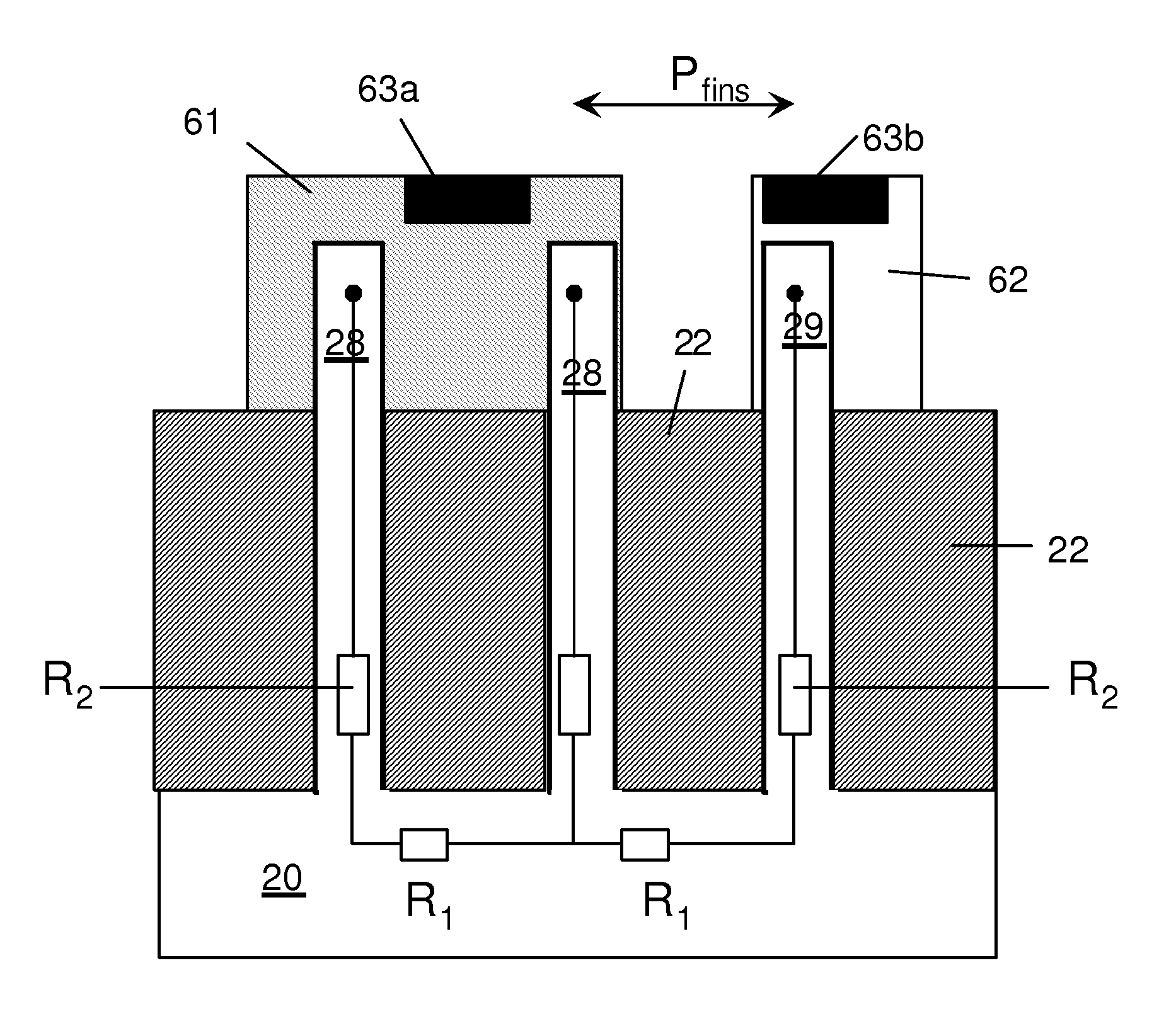
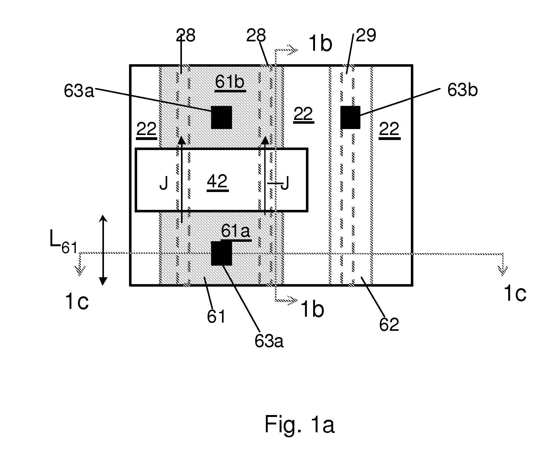
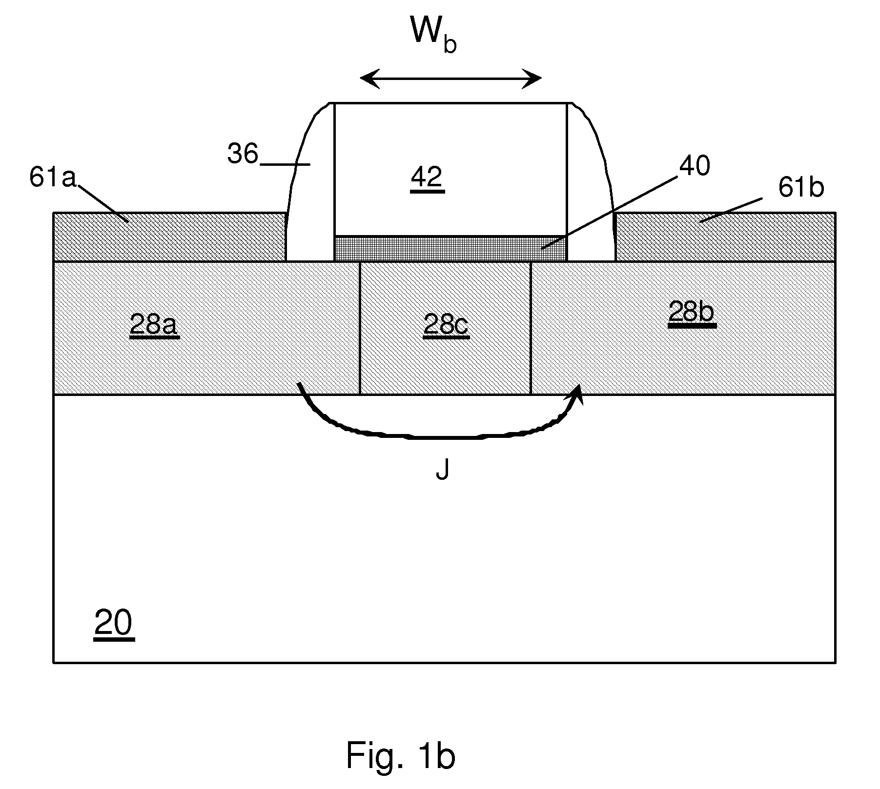
[0019]While non-planar devices, such as multi gate devices or FINFET devices, have been offered for future technologies to mitigate problems with scaling planar CMOS technologies, such multiple gate designs create challenges in designing and forming other devices such as bipolar devices. Unlike planar technologies, where gate l...


PUM


Abstract

Design and methods for fabricating bipolar junction transistors are described. In one embodiment, a semiconductor device includes a first fin comprising a first emitter region, a first base region, and a first collector region. The first emitter region, the first base region, and the first collector region form a bipolar junction transistor. A second fin is disposed adjacent and parallel to the first fin. The second fin includes a first contact to the first base region.

Description

[0001]This application claims the benefit of U.S. Provisional Application No. 61 / 147,980 filed on Jan. 28, 2009, entitled “Bipolar Junction Transistors and Methods of Fabrication Thereof,” which application is hereby incorporated herein by reference.TECHNICAL FIELD[0002]The present invention relates generally to semiconductor devices, and more particularly, to designs and methods of fabrication of bipolar junction transistors.BACKGROUND[0003]Semiconductor devices are used in a large number of electronic devices, such as computers, cell phones, and others. Semiconductor devices comprise integrated circuits that are formed on semiconductor wafers by depositing many types of thin films of material over the semiconductor wafers, and patterning the thin films of material to form the integrated circuits. Integrated circuits include field-effect transistors (FETs) such as metal oxide semiconductor (MOS) transistors.[0004]One of the goals of the semiconductor industry is to continue shrinki...

Claims


Application Information

Patent Timeline
Patent Type & Authority Applications(United States)
IPC IPC(8): H01L29/73
CPCH01L29/73H01L21/823431
Inventor KE, PO-YAOCHUNG, TAO-WENCHUNG, SHINEHSUEH, FU-LUNG
Owner TAIWAN SEMICON MFG CO LTD
Why Eureka
Try Eureka