Power-supply wiring structure for multilayer wiring and method of manufacturing multilayer wiring

a technology of power-supply wiring and multi-layer wiring, which is applied in the direction of electrical equipment, semiconductor devices, semiconductor/solid-state device details, etc., can solve the problems of deteriorating the wiring property of signal wires

Inactive Publication Date: 2010-09-23
KK TOSHIBA
View PDF3 Cites 31 Cited by
  • Summary
  • Abstract
  • Description
  • Claims
  • Application Information

AI Technical Summary

Problems solved by technology

However, in such a method of connecting between power supply wires, the connecting wires occupy wiring tracks for signal wires in the intermediate wiring layers present between the two power supply wires.
Therefore, a wiring property of the signal wires is deteriorated.

Method used


Image

  • Power-supply wiring structure for multilayer wiring and method of manufacturing multilayer wiring
  • Power-supply wiring structure for multilayer wiring and method of manufacturing multilayer wiring
  • Power-supply wiring structure for multilayer wiring and method of manufacturing multilayer wiring

Examples


Embodiment Construction

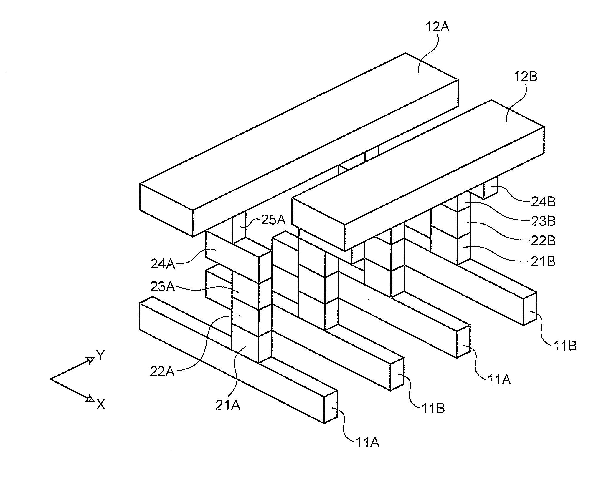
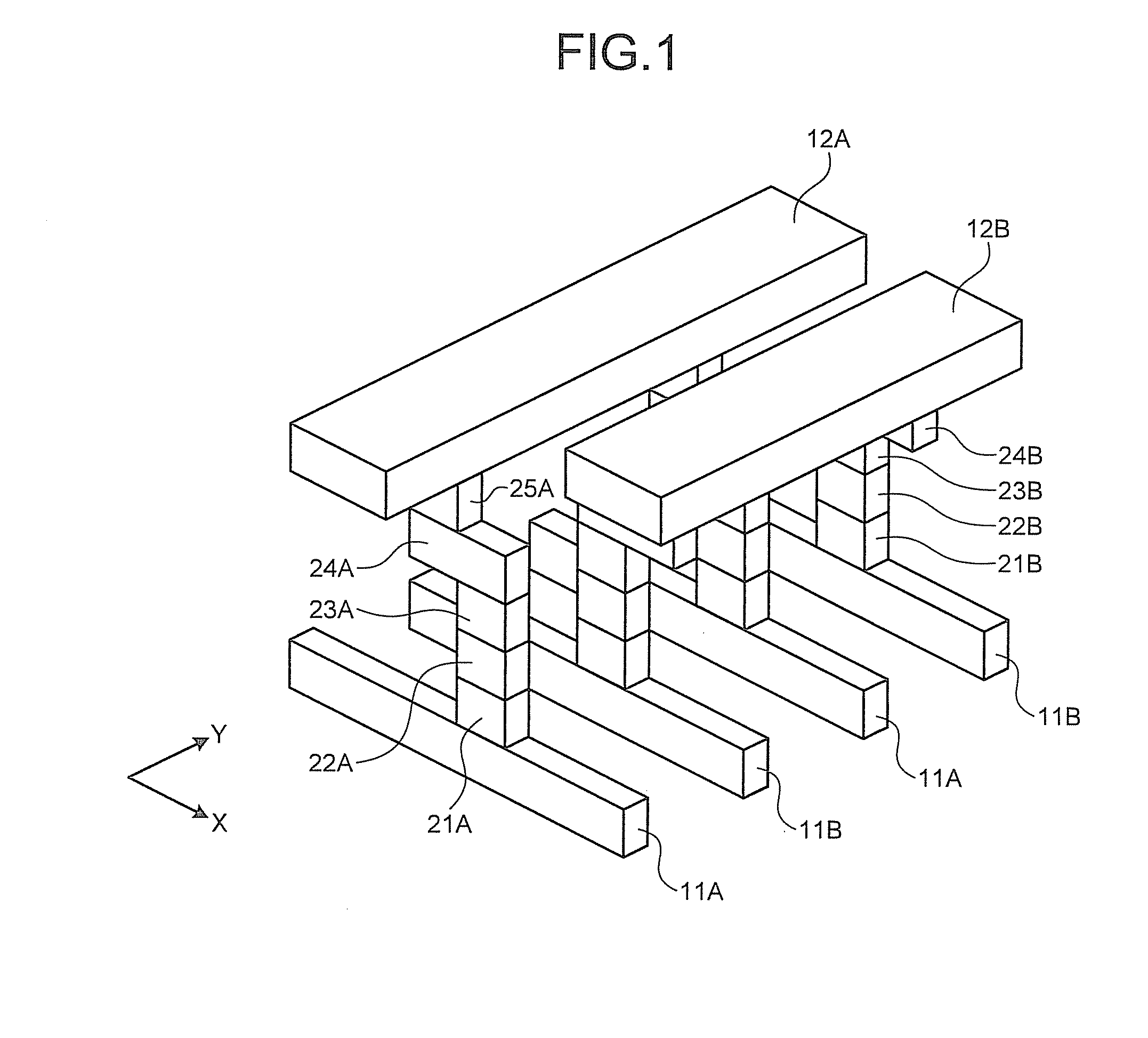
[0025]Exemplary embodiments of the present invention are explained in detail below with reference to the accompanying drawings. In the embodiments, a power-supply wiring structure in a multilayer wiring structure of a semiconductor integrated circuit is explained as an example. However, the present invention is not limited by the embodiments. Perspective views and sectional views of the multilayer wiring of the semiconductor integrated circuit used in the embodiments are schematic. A relation between the thickness and the width of a layer, a ratio of the thicknesses of layers, and the like are different from actual ones.

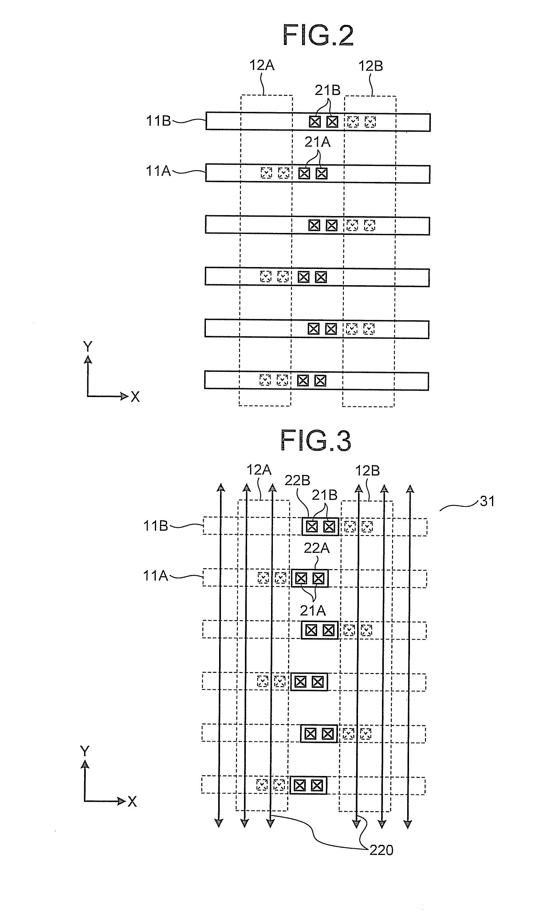
[0026]FIG. 1 is a schematic perspective view of an example of a power-supply wiring structure for a multilayer wiring in a semiconductor integrated circuit according to an embodiment of the present invention. FIG. 2 is a plan view of a lower-layer power-supply wiring layer shown in FIG. 1. FIG. 3 is a plan view of a first intermediate wiring layer shown in FIG. 1. FI...


PUM


Abstract

A power-supply wiring structure for a multilayer wiring according to an embodiment of the present invention includes one intermediate wiring layer with a first direction set as a priority wiring direction including a position converting and connecting wire, which has crossing-position forming sections formed in crossing positions of upper-layer power supply wires and lower-layer power supply wires of the same kind and projecting sections projecting from the crossing-position forming sections to sides of upper-layer power supply wires of different kinds, and includes a wire connecting section that connects between the upper layer wires and the crossing-position forming section and connects between the projecting section and the lower layer wires via vias.

Description

CROSS-REFERENCE TO RELATED APPLICATIONS[0001]This application is based upon and claims the benefit of priority from the prior Japanese Patent Application No. 2009-064839, filed on Mar. 17, 2009; the entire contents of which are incorporated herein by reference.BACKGROUND OF THE INVENTION[0002]1. Field of the Invention[0003]The present invention relates to a power-supply wiring structure for a multilayer wiring and a method of manufacturing the multilayer wiring.[0004]2. Description of the Related Art[0005]In general, in a semiconductor integrated circuit, in connecting between two power supply wires which are crossed each other and arranged at wiring layers separated in the vertical direction across intermediate wiring layers, a method of forming a connecting section by arranging, in a crossing area of the two power supply wires, stacked vias superimposed across connecting wires formed in the intermediate wiring layers to thereby connect between the two power supply wires is widely ...

Claims


Application Information

Patent Timeline
Patent Type & Authority Applications(United States)
IPC IPC(8): H01L23/48H01L21/768
CPCH01L23/5286H01L2924/0002H01L2924/00
Inventor UTSUMI, TETSUAKI
Owner KK TOSHIBA
Why Eureka
Try Eureka