Directional coupler

a technology of directional couplers and coupling lines, applied in the direction of coupling devices, electrical devices, waveguides, etc., can solve the problems of manufacturing variations, significant increase in reflection loss in chips, degradation of reflection loss characteristics of coupled lines, etc., and achieve good reflection loss characteristics

Active Publication Date: 2011-03-10
MURATA MFG CO LTD
View PDF3 Cites 63 Cited by
  • Summary
  • Abstract
  • Description
  • Claims
  • Application Information

AI Technical Summary

Benefits of technology

[0016]When the directional coupler of the present invention is mounted, e.g., on a module substrate so that the coupled port and the isolated port of the coupler are connected to the module substrate by connecting members, the first and second capacitive elements of the directional coupler are electric

Problems solved by technology

As shown in FIG. 22, the addition of the wires (which have an inductance) to the chip results in a significant increase in the reflection loss in the chip.
The degradation of the reflection loss characteristics of the coupled line as shown in FIG. 22 presents a problem when the coupled lines of several directional couplers are connected in series, as shown in FIG. 19, to achieve multiband capability.
This degradation of the combined reflection loss characteristics will result in manufacturing v

Method used


Image

  • Directional coupler
  • Directional coupler
  • Directional coupler

Examples


first embodiment

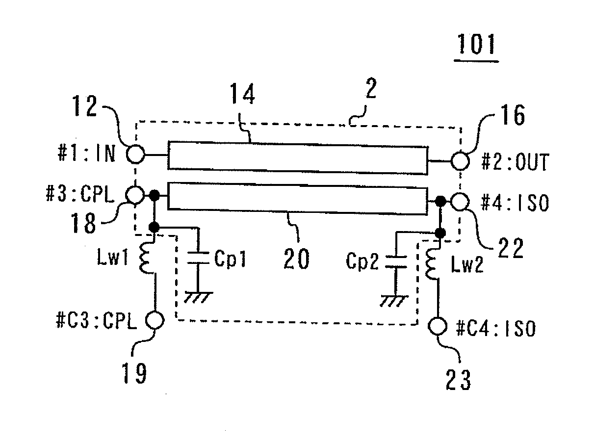
[0039]Preferred embodiments of the present invention will be described in connection with a configuration in which a chip with a directional coupler thereon is mounted on a module substrate or a printed board. The chip with a directional coupler thereon can be manufactured by a GaAs-HBT process, a GaAs-BiFET (HBT+FET or HBT+HEMT) process, or a GaAs-HEMT / FET process. The coupled port and the isolated port of the directional coupler are both connected to a component or device outside the module. This connection is accomplished through inductive connecting elements, such as bonding wires, and transmission lines in the module substrate. It should be noted that the embodiments described below can also be applied to directional couplers manufactured by a Si-based process. Further, these embodiments are suitable as applied to the case where the coupled lines (also referred to as the “sub-lines”) of the directional couplers in a multiband-capable terminal are connected in series with one an...

second embodiment

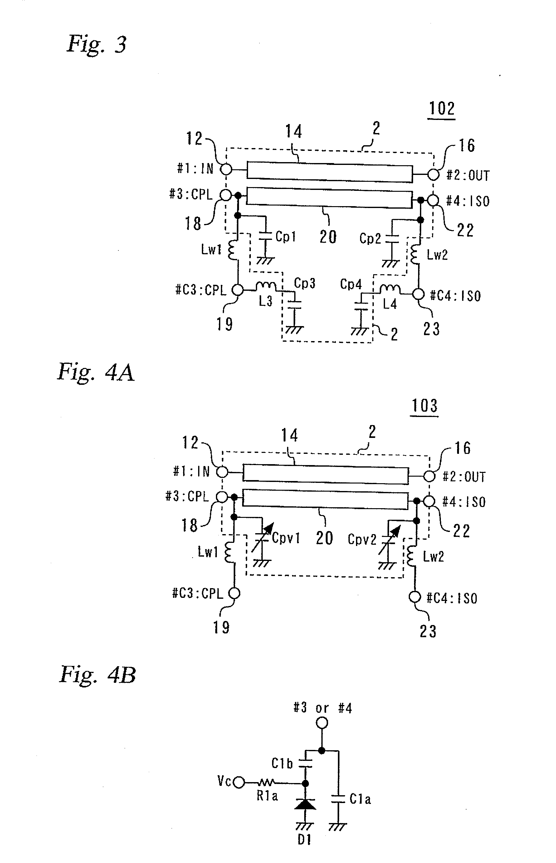
[0047]FIG. 3 is a circuit diagram of a directional coupler 102 according to a second embodiment of the present invention. This directional coupler 102 differs from the directional coupler 101 of the first embodiment in that it additionally includes inductances L3 and L4 and capacitive elements Cp3 and Cp4. L3 and L4 are the parasitic inductances of connecting elements. That is, each matching circuit to the coupled line 20 of the directional coupler 102 is an LCLC circuit and includes 4 components, whereas each matching circuit to the coupled line of the directional coupler 101 of the first embodiment shown in FIG. 1 is an LC circuit and includes 2 components. This increase in the number of components allows the reflection loss characteristics of the coupled line to be improved over a wider band, as compared with the first embodiment.

third embodiment

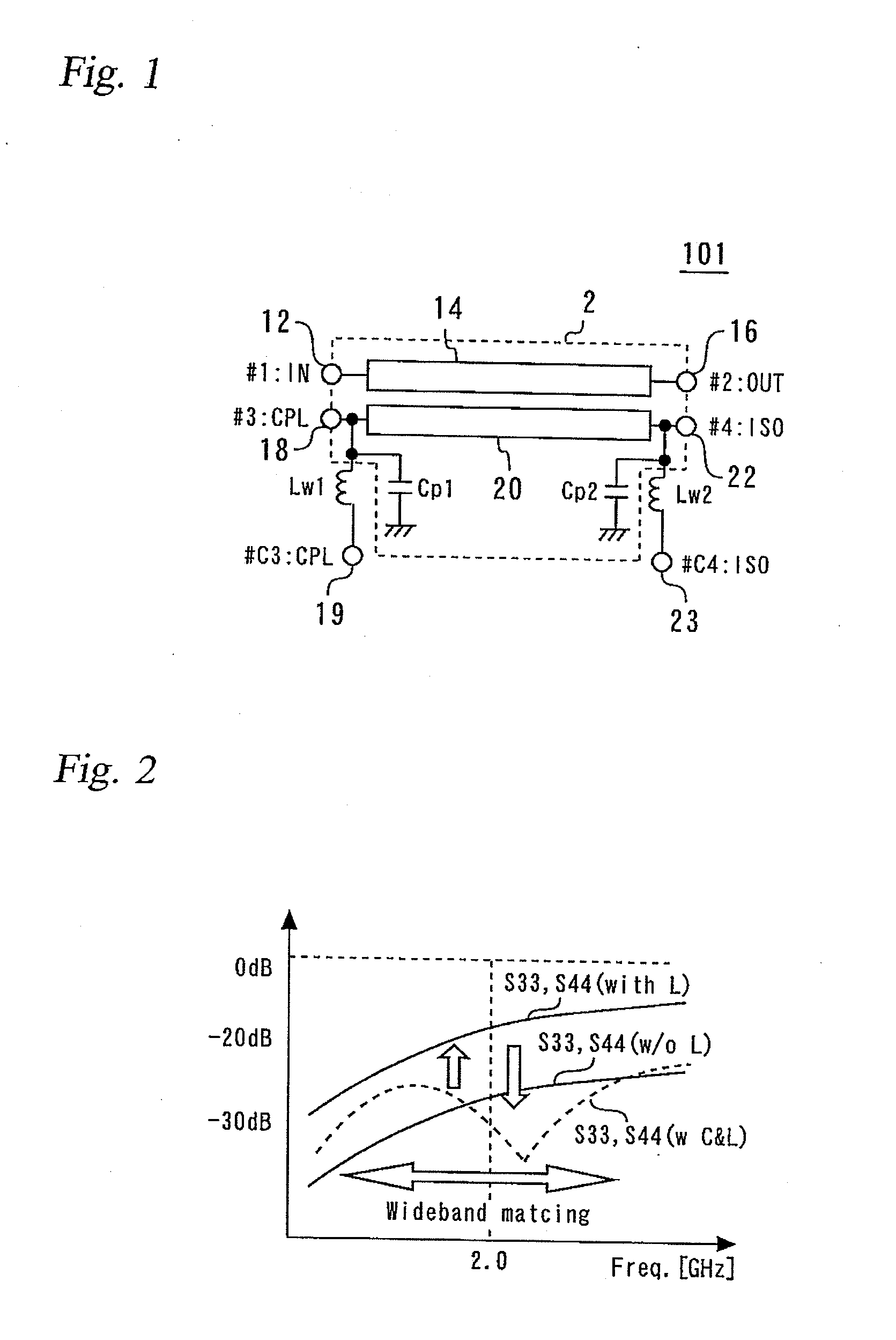
[0048]FIG. 4, which includes FIGS. 4A and 4B, is a circuit diagram of a directional coupler 103 according to a third embodiment of the present invention. This directional coupler 103 differs from the directional coupler 101 shown in FIG. 1 in that the capacitive elements Cp1 and Cp1 are replaced by variable capacitance elements Cpv1 and Cpv2, respectively, as shown in FIG. 4A. FIG. 4B shows the actual circuit configuration of the variable capacitance elements Cpv1 and Cpv2. As shown in FIG. 4B, each of Cpv1 and Cpv2 includes a resistance R1a, a capacitance Cb1, a variable capacitance diode D1, and a fixed value capacitance C1a. The capacitance of Cpv1 and Cpv2 can be varied by varying the control voltage Vc. This makes it possible to vary the reflection characteristics of the coupled line (which characteristics correspond to those indicated by the reference symbol “S33, S44 (w-C&L)” in FIG. 2), allowing the characteristics to be adjusted finely or over a selected band even after mou...


PUM


Abstract

A directional coupler includes capacitive elements electrically connected to a coupled port and an isolated port, respectively, for a coupled line on a chip (on-chip). The capacitive elements serve as matching capacitive elements and may be MIM (Metal Insulator Metal) capacitors on a substrate. A first end of a first of the capacitive elements is connected between the coupled port and the coupled line and a second end is grounded. A first end of a second of the capacitive elements is connected between the isolated port and the coupled line and a second end is grounded.

Description

FIELD OF THE INVENTION[0001]The present invention relates to a directional coupler.BACKGROUND ART[0002]Directional couplers have been used in various applications. FIG. 17 shows an exemplary application of a directional coupler, specifically, a typical system in a cellular phone unit which includes a power amplifier (or PA), a directional coupler, and a wave detecting circuit. The reference symbol ANT denotes an antenna. The system shown in FIG. 17 is adapted to monitor power through the directional coupler. In this system, the forward power from the PA can be accurately monitored by greatly reducing the influence of the mismatch in impedance at the antenna terminal on the detected voltage by virtue of the directivity of the directional coupler. Such monitoring systems are often used in GSM (Global System for Mobile Communications) terminals, which are widely used overseas, and in CDMA terminals. However, they are not limited to use in terminals, but are the most common systems for ...

Claims


Application Information

Patent Timeline
IPC IPC(8): H01P5/18
CPCH01P5/184H01P5/18
Inventor YAMAMOTO, KAZUYAMIYASHITA, MIYOKURUSU, HITOSHIASADA, TOMOYUKI
Owner MURATA MFG CO LTD
Why Eureka
Try Eureka