Semiconductor light receiving device
- Summary
- Abstract
- Description
- Claims
- Application Information
AI Technical Summary
Problems solved by technology
Method used
Image

Examples
first embodiment
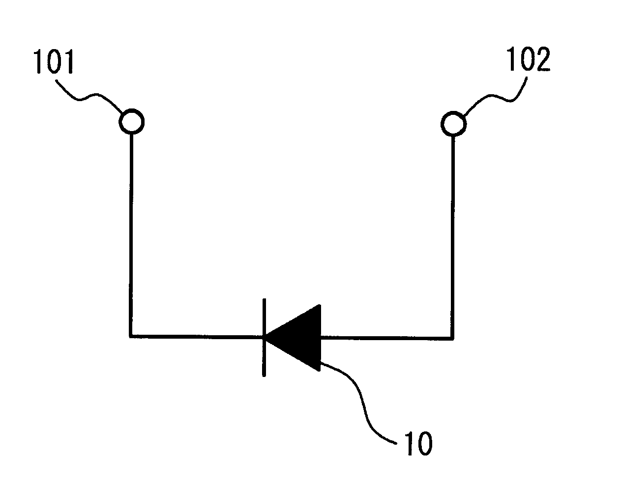
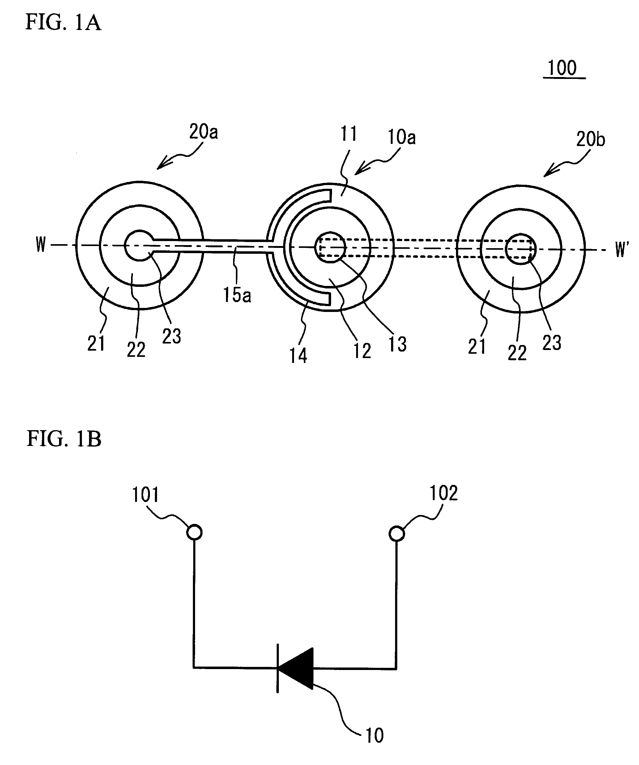
FIG. 1A illustrates a plane view of a mesa included in a semiconductor light receiving device 100 in accordance with a first embodiment. As illustrated in FIG. 1A, the semiconductor light receiving device 100 includes a semiconductor light receiving element 10a and dummy mesas 20a and 20b. The semiconductor light receiving element 10a and the dummy mesas 20a and 20b are mounted on a semi-insulating semiconductor substrate 50 described later. The semiconductor light receiving element 10a and the dummy mesas 20a and 20b have a mesa shape. The semiconductor light receiving device 100 includes a carrier 40 described later. In FIG. 1A, a carrier wiring of the carrier 40 is illustrated with a dotted line.
As illustrated in FIG. 1A, the semiconductor light receiving element 10a has a structure in which an upper mesa 12 and an upper electrode 13 are provided on a lower mesa 11 in this order. For example, the lower mesa 11 has a cylinder shape. The upper mesa 12 has a cylinder shape having a ...
modified embodiment
FIG. 3 illustrates a modified embodiment of the first embodiment. As illustrated in FIG. 3, there may be provided a mesa-shaped device 60 including a passive element such as a capacitor and a resistor instead of the dummy mesa 20b. In this case, applying high electrical field to the insulating layer 35 provided on the surface of the semiconductor light receiving element 10a is restrained if a carrier wiring coupling the upper electrode 13 of the semiconductor light receiving element 10a and an upper electrode of another device 60. In the modified embodiment, the mesa-shaped device 60 acts as the second mesa.
second embodiment
A second embodiment is a case where two semiconductor light receiving elements are provided on the semi-insulating semiconductor substrate 50. FIG. 4A illustrates a plane view of a mesa included in a semiconductor light receiving device 100a in accordance with the second embodiment. As illustrated in FIG. 4A, the semiconductor light receiving device 100a includes the semiconductor light receiving elements 10a and 10b and the dummy mesas 20a and 20b. The semiconductor light receiving elements 10a and 10b and the dummy mesas 20a and 20b are formed on the semi-insulating semiconductor substrate 50 and have a mesa shape. The semiconductor light receiving element 10b has the same structure as the semiconductor light receiving element 10a. In FIG. 4A, a carrier wiring of the carrier 40 are illustrated with a dotted line.
As illustrated in FIG. 4A, the dummy mesa 20a, the semiconductor light receiving element 10a, the dummy mesa 20b and the semiconductor light receiving element 10b are alig...
PUM
 Abstract
Description
Claims
Application Information
 - R&D Engineer
- R&D Manager
- IP Professional
- Industry Leading Data Capabilities
- Powerful AI technology
- Patent DNA Extraction
Browse by: Latest US Patents, China's latest patents, Technical Efficacy Thesaurus, Application Domain, Technology Topic.
© 2024 PatSnap. All rights reserved.Legal|Privacy policy|Modern Slavery Act Transparency Statement|Sitemap