Cross-hair cell based floating body device

a floating body, cross-hair cell technology, applied in the direction of semiconductor devices, basic electric elements, electrical equipment, etc., can solve the problems of increasing difficulty in building gates or other structures of fins, and difficulty in construction

Active Publication Date: 2011-08-11
MICRON TECH INC
View PDF1 Cites 35 Cited by
  • Summary
  • Abstract
  • Description
  • Claims
  • Application Information

AI Technical Summary

Problems solved by technology

High aspect ratio fins typically are desirable but challenging to construct.
As the dimensions of the fin structures and the space between each fin are reduced, construction of gates or other structures of the fins may be increasingly difficult.

Method used


Image

  • Cross-hair cell based floating body device
  • Cross-hair cell based floating body device
  • Cross-hair cell based floating body device

Examples


Embodiment Construction

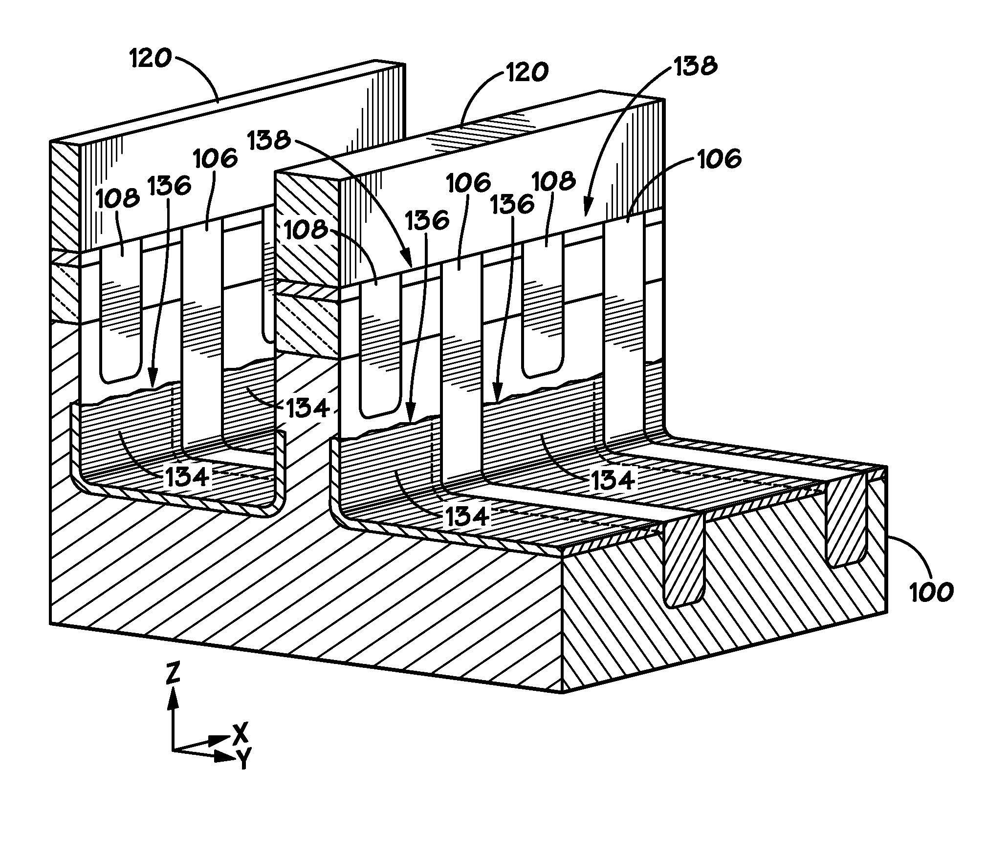
[0015]Some of the subsequently discussed embodiments may facilitate the manufacture of high aspect ratio structures, such as finFETs. As is described in detail below, during manufacture of the finFET, a hollow region may be formed during etch of the sidewalls of the fins. An oxide or other suitable material may be formed in the hollow region to isolate portions of the transistor from a substrate. The resulting structures may form a floating body cell in the body of the fin. The following discussion describes devices and process flows in accordance with embodiments of the present technique. Prior to addressing these embodiments from the device and process flow perspective, systems in accordance with embodiments of the present technique are described.

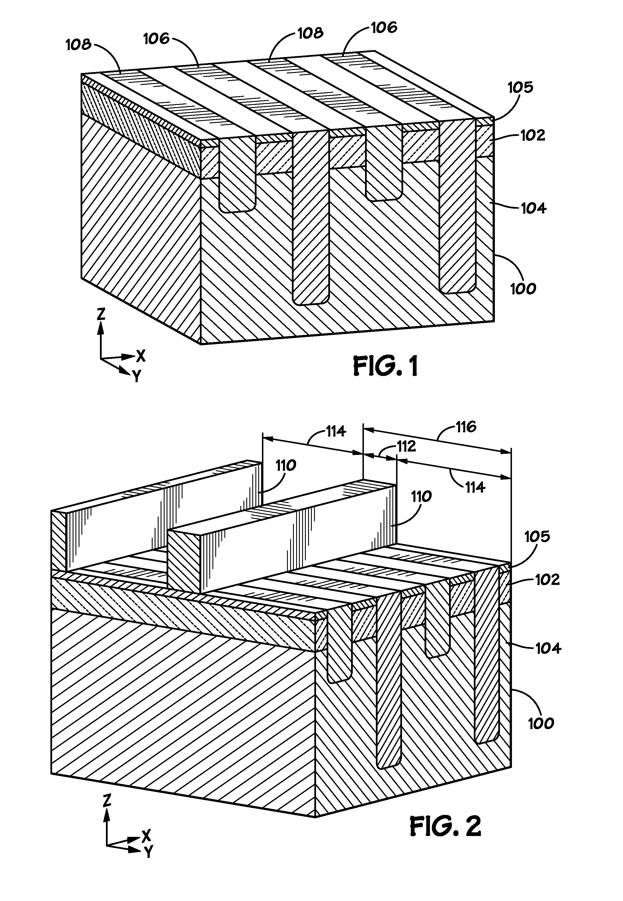
[0016]FIG. 1 depicts a substrate 100 having features formed during a manufacturing process in accordance with an embodiment of the present invention. It should be appreciated that the features described below in FIG. 1 may be formed by an...


PUM


Abstract

A non-planar transistor having floating body structures and methods for fabricating the same are disclosed. In certain embodiments, the transistor includes a fin having upper and lower doped regions. The upper doped regions may form a source and drain separated by a shallow trench formed in the fin. During formation of the fin, a hollow region may be formed underneath the shallow trench, isolating the source and drain. An oxide may be formed in the hollow region to form a floating body structure, wherein the source and drain are isolated from each other and the substrate formed below the fin. In some embodiments, independently bias gates may be formed adjacent to walls of the fin. In other embodiments, electrically coupled gates may be formed adjacent to the walls of the fin.

Description

BACKGROUND[0001]1. Field of Invention[0002]The invention relates generally to electronic devices, and, more specifically, to non-planar transistors and techniques for fabricating the same.[0003]2. Description of Related Art[0004]Fin field effect transistors (finFETs) are often built around a fin (e.g., a tall, thin semiconductive member) extending generally perpendicularly from a substrate. Typically, a gate traverses the fin by conformally running up one side of the fin over the top and down the other side of the fin. Generally, a source and a drain are located on opposite sides of the gate in the fin. In operation, a current through the fin between the source and drain is controlled by selectively energizing the gate.[0005]High aspect ratio fins typically are desirable but challenging to construct. Generally, high aspect ratio finFETS can be integrated into a small area of the substrate, thereby potentially reducing manufacturing costs on a per-transistor basis. To increase densit...

Claims


Application Information

Patent Timeline
Patent Type & Authority Applications(United States)
IPC IPC(8): H01L29/78H01L21/762
CPCH01L27/10802H01L29/785H01L29/7841H01L27/10826H10B12/20H10B12/36
Inventor JUENGLING, WERNER
Owner MICRON TECH INC
Why Eureka
Try Eureka