Display panel

Active Publication Date: 2011-09-08
LAPIS SEMICON CO LTD
View PDF13 Cites 7 Cited by
  • Summary
  • Abstract
  • Description
  • Claims
  • Application Information

AI Technical Summary

Benefits of technology

[0010]The present invention provides a display panel that may suppress increase in area of a driver IC due to increased numbers of input terminals.
[0013]Therefore, according to the first aspect of the present invention, the number of input terminals that can be disposed may increase, since the input terminals are disposed along the first long side in the driver IC, when compared with, for example, a case where the first input terminal group is disposed along the first short side in the driver IC. Moreover, the first aspect of the present invention may suppress the increase in area of the driver IC due to increased number of input terminals.
[0019]According to the above aspect, when compared with, for example, a case where the first input terminal group is disposed along the first short side of the driver IC, the number of input terminals that can be disposed may be increased, since the width of the wiring in the first wiring group is smaller than width of each terminal. Accordingly, the above aspect of the present invention may suppress the increase in area of the driver IC due to increased number of input terminals.
[0021]According to the above aspect, when compared with, for example, a case where the first input terminal group is disposed along the first short side of the driver IC, the number of input terminals that can be disposed may be increased, since the interval between the wirings in the first wiring group is smaller than the interval between the terminals in the first input terminal group. Accordingly, the above aspect of the present invention may suppress the increase in area of the driver IC due to increased number of input terminals.
[0030]According to the above aspects, the present invention provides a display panel that may suppress increase in area of a driver IC due to increased numbers of input terminals.

Problems solved by technology

Therefore, the above configuration cannot be applied to a display panel that has no wiring interposed between a panel end portion and the driver IC.

Method used


Image

  • Display panel
  • Display panel
  • Display panel

Examples


Embodiment Construction

[0038]Hereinbelow, a description will be given of a display panel according to an exemplary embodiment of the present invention with reference to the attached drawings. Note that constituent elements having substantially the same functions will be designated by the same reference numerals throughout the drawings, and their explanations may be omitted.

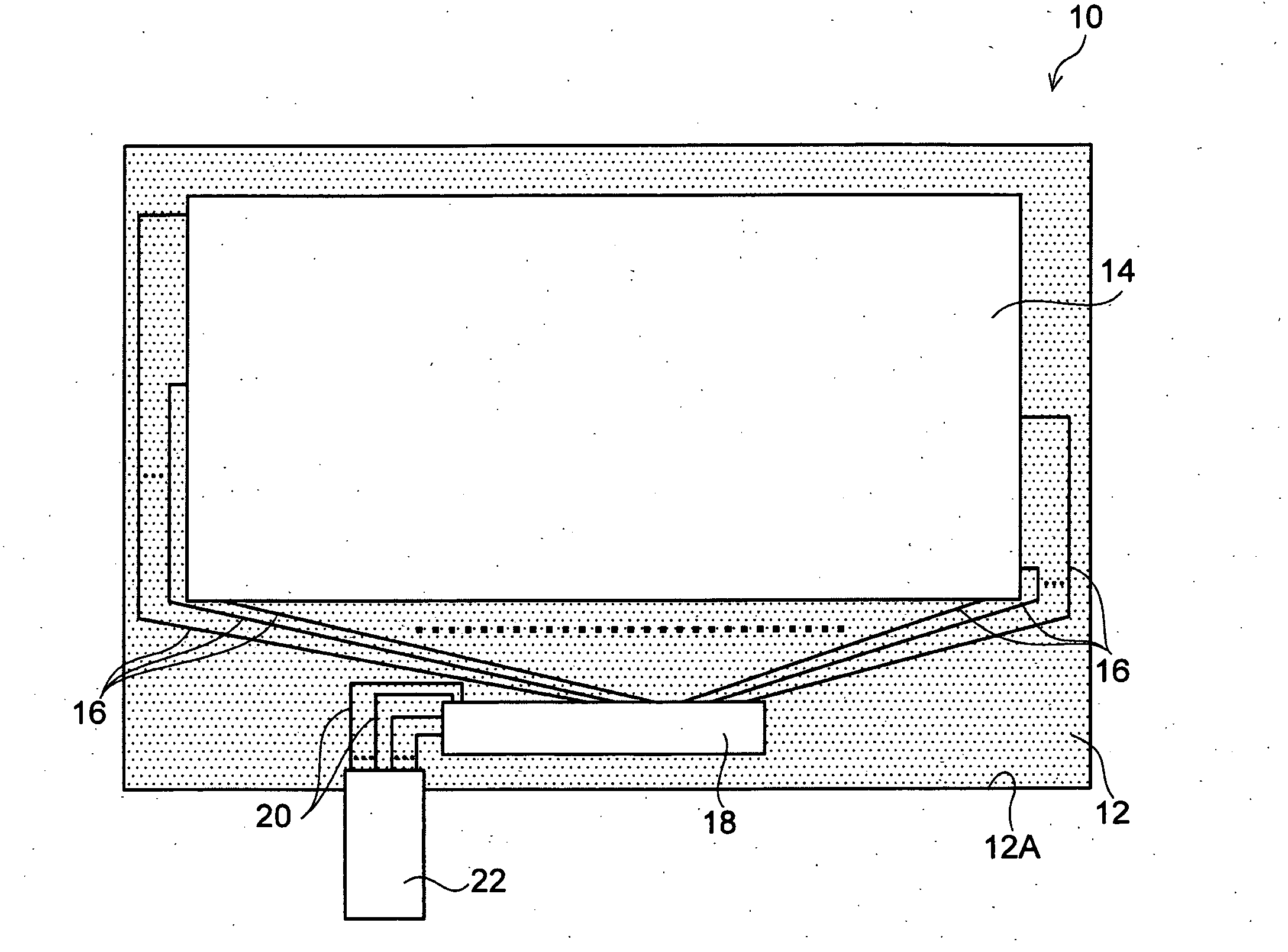
[0039]FIG. 1 is a view showing the schematic configuration of a display panel according to an exemplary embodiment of the invention.

[0040]A display panel 10 of the exemplary embodiment according to the present invention includes a panel body 12 formed into a rectangular shape when viewed from the front. At substantially the center of the panel body 12, a rectangular display section 14 is disposed so that a longitudinal direction of the rectangular display section 14 matches with a longitudinal direction of the panel body 12.

[0041]One end of each transparent electrode 16, wired to the panel body 12, is connected to the display section 14...


PUM


Abstract

The present invention provides a display panel including: a first input terminal group in which input terminals are disposed at intervals along first long side of a rectangular driver IC facing a panel end portion; a second input terminal group in which input terminals are disposed at intervals along the second long side of the driver IC facing a display section; a first wiring group connected to the first input terminal group, that extends under the first short side of the driver IC and extends out from between the driver IC and the panel body; and a second wiring group connected to the second input terminal group, that passes under the second long side of the driver IC and extends out from between the driver IC and the panel body.

Description

Cross-Reference to Related Application[0001]This application claims priority under 35 USC 119 from Japanese Patent Application No. 2010-049657, filed on Mar. 5, 2010, the disclosure of which is incorporated by reference herein.BACKGROUND OF THE INVENTION[0002]1. Field of the Invention[0003]The present invention relates to a display panel.[0004]2. Description of the Related Art[0005]A conventional display panel that has narrowed frame by not providing groups of wirings including transparent electrodes provided between a panel end portion of a panel body and a driver IC for driving a display unit, so as to reduce an interval defined between the panel end portion and the driver IC, has been known.[0006]Input terminals of the driver IC are normally disposed along a first short side of the driver IC. However, when the number of input terminals is large, and the input terminals cannot be disposed along the first short side, the input terminals may be disposed along the first long side of ...

Claims


Application Information

Patent Timeline
IPC IPC(8): H05K7/00
CPCH05K7/00G02F1/13452H05K3/361G02F1/1345G09G2300/0426G02F1/13456G09G3/20G09G3/3648G09G2300/0408G09G5/003G09G2354/00
Inventor OHNO, TAKASHIIMAYOSHI, TAKAHIROKAWAGOE, MASAKUNI
Owner LAPIS SEMICON CO LTD
Why Eureka
Try Eureka