
Package for a wireless enabled integrated circuit

Inactive Publication Date: 2011-12-29
AVAGO TECH WIRELESS IP SINGAPORE PTE
View PDF33 Cites 5 Cited by
  • Summary
  • Abstract
  • Description
  • Claims
  • Application Information

AI Technical Summary

Benefits of technology

[0011]These and other advantages and features will become readily apparent in view of the following detailed description of the invention. Note that the Summary and Abstract sections may set forth one or more, but not all exemplary embodiments of the present invention as contemplated by the inventor(s).

Problems solved by technology

Conventional ways of coupling an IC die to a substrate can, however, be costly.
For example, the materials used to create wirebonds, e.g., gold, can be expensive, thus increasing the cost of the entire device.
Furthermore, the conventional ways of coupling the IC die to the substrate can also be susceptible to manufacturing defects.
For example, wirebonds and / or solder bumps can break or be damaged during the manufacturing process, reducing the throughput for the IC device.

Method used


Image

  • Package for a wireless enabled integrated circuit
  • Package for a wireless enabled integrated circuit
  • Package for a wireless enabled integrated circuit

Examples


Embodiment Construction

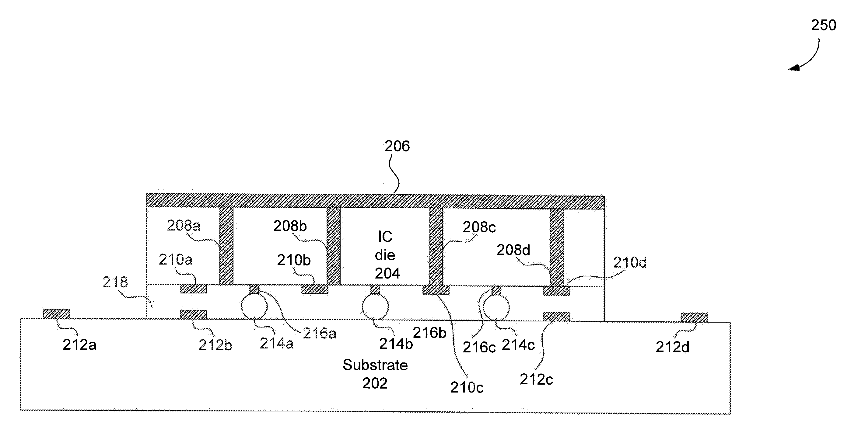
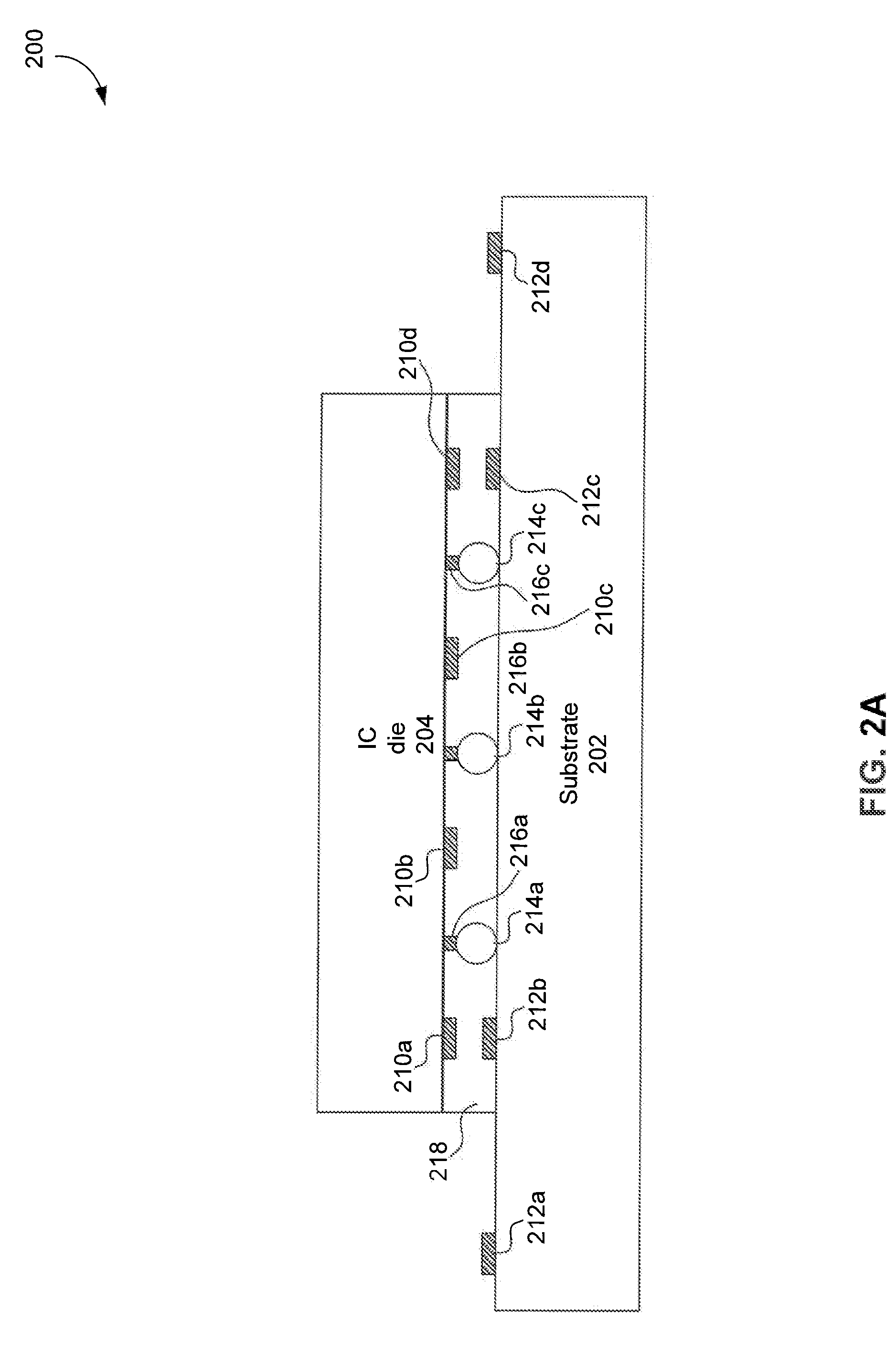
[0022]References in the specification to “one embodiment”, “an embodiment”, “an example embodiment”, etc., indicate that the embodiment described may include a particular feature, structure, or characteristic, but every embodiment may not necessarily include the particular feature, structure, or characteristic. Moreover, such phrases are not necessarily referring to the same embodiment. Further, when a particular feature, structure, or characteristic is described in connection with an embodiment, it is submitted that it is within the knowledge of one skilled in the art to effect such feature, structure, or characteristic in connection with other embodiments whether or not explicitly described.

[0023]Furthermore, it should be understood that spatial descriptions (e.g., “above”, “below”, “left,”“right,”“up”, “down”, “top”, “bottom”, etc.) used herein are for purposes of illustration only, and that practical implementations of the structures described herein can be spatially arranged in...


PUM


Abstract

An integrated circuit (IC) device is provided. The IC device includes a substrate, an IC die coupled to the substrate, and a first wirelessly enabled functional block formed on the IC die. The first wirelessly enabled functional block is configured to wirelessly communicate with a second wirelessly enabled functional block formed on the substrate.

Description

CROSS REFERENCE TO RELATED APPLICATIONS[0001]This application claims the benefit of U.S. Provisional Appl. No. 61 / 357,880, filed Jun. 23, 2010, which is incorporated by reference herein in its entirety.BACKGROUND OF THE INVENTION[0002]1. Field of the Invention[0003]The present invention generally relates to integrated circuit (IC) devices, and more particularly to connections between elements of an IC device.[0004]2. Background Art[0005]Integrated circuit (IC) devices typically include an IC die housed in a package. The IC device can be coupled to a printed circuit board (PCB) to enable communication between the IC device and other devices coupled to the PCB. For example, in array-type packages, an IC die is often coupled to a substrate, which is coupled to an array of connection elements, e.g., an array of solder balls. The array of connections elements is then physically coupled to the PCB.[0006]An IC die can be coupled to a substrate in a variety of ways. For example, in die-down...

Claims


Application Information

Patent Timeline
IPC IPC(8): H01L23/48H01L21/60
CPCH01L23/48H01L23/522H01L2924/3025H01L23/66H01L2223/6677H01L2224/16225H01L2224/32225H01L2224/48227H01L2224/73204H01L2224/73253H01L2224/73265H01L2924/15311H01L2924/16251H01L2924/00012H01L2924/00H01L24/73H01L2924/14
Inventor ZHAO, SAM ZIQUNROFOUGARAN, AHMADREZABEHZAD, ARYACASTANEDA, JESUSBOERS, MICHAEL
Owner AVAGO TECH WIRELESS IP SINGAPORE PTE
Features
  • Generate Ideas
  • Intellectual Property
  • Life Sciences
  • Materials
  • Tech Scout
  • Unparalleled Data Quality
  • Higher Quality Content
  • 60% Fewer Hallucinations
Learn More