Power converter

a technology of power converters and cooling fins, applied in power conversion systems, ac-dc conversion, electrical apparatus, etc., can solve the problems of too high cooling capability of cooling fins, and achieve the effect of equalizing the loss occurring in semiconductor devices

Active Publication Date: 2012-09-13
FUJI ELECTRIC CO LTD
View PDF7 Cites 8 Cited by
  • Summary
  • Abstract
  • Description
  • Claims
  • Application Information

AI Technical Summary

Benefits of technology

[0014]Embodiments of the present invention address these and other needs. Embodiments of the invention provide a power converter with which it is possible to equalize the loss occurring in semiconductor devices.
[0021]According to embodiments of the invention, it is possible to provide a power converter with which it is possible to equalize the loss occurring in semiconductor devices.

Problems solved by technology

Because of this, when considering the cooling of the semiconductor device M20, the cooling capability of the cooling fin is too high.

Method used


Image

  • Power converter
  • Power converter
  • Power converter

Examples


first embodiment

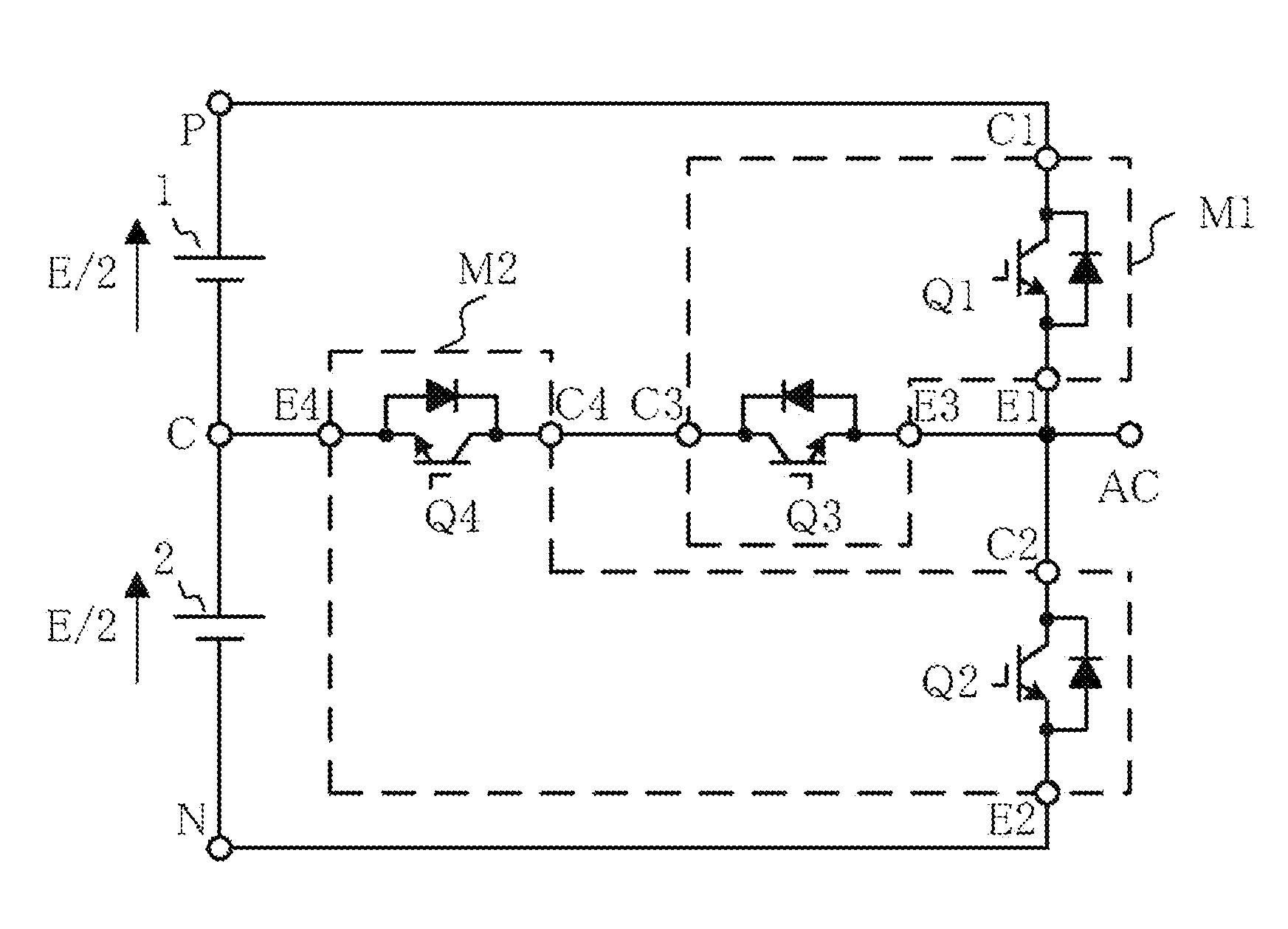
[0032]FIG. 1 is a diagram for illustrating the power converter according to the invention.

[0033]In FIG. 1, the semiconductor device M1 has four terminals, terminals C1, E1, C3, and E3, for connecting to an external circuit. The terminal C1 is connected to the collector terminal of the semiconductor switching element Q1, while the terminal E1 is connected to the emitter terminal. Also, the terminal C3 is connected to the collector terminal of the semiconductor switching element Q3, while the terminal E3 is connected to the emitter terminal. Then, the collector terminal and the emitter terminal of the semiconductor switching element Q1 and the collector terminal and the emitter terminal of the semiconductor switching element Q3 are each isolated.

[0034]Meanwhile, the semiconductor device M2 has four terminals, terminals C2, E2, C4, and E4, for connecting to an external circuit. The terminal C2 is connected to the collector terminal of the semiconductor switching element Q2, while the t...

second embodiment

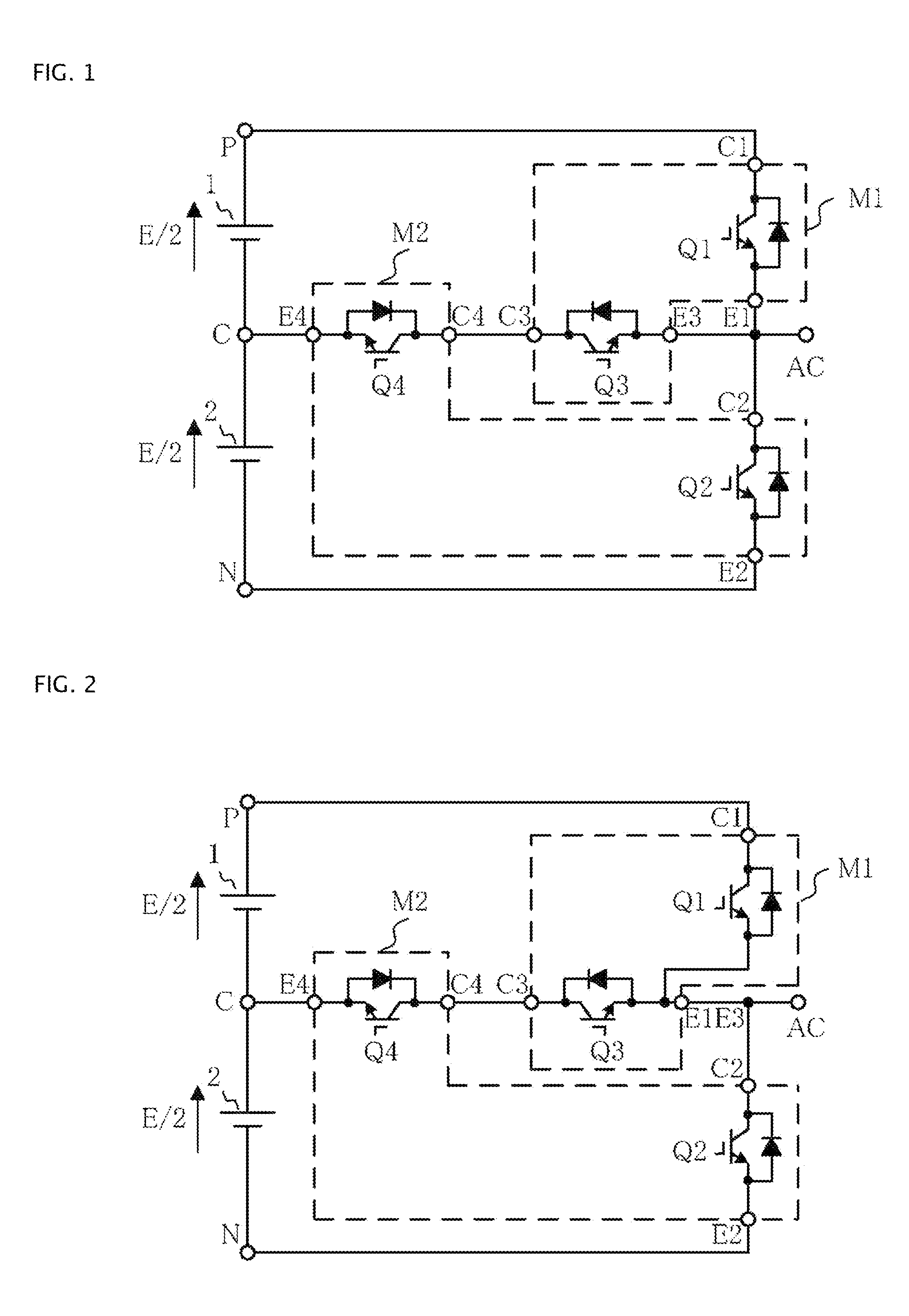
[0038]FIG. 2 is a diagram for illustrating the power converter according to the invention.

[0039]In FIG. 2, the semiconductor device M1 has three terminals, terminals C1, E1E3, and C3, for connecting to an external circuit. The terminal C1 is connected to the collector terminal of the semiconductor switching element Q1, while the terminal C3 is connected to the collector terminal of the semiconductor switching element Q3. Then, the emitter terminal of the semiconductor switching element Q1 and the emitter terminal of the semiconductor switching element Q3 are connected inside the semiconductor device M1. This connection point is connected to the terminal E1E3 for connection to an external circuit.

[0040]Meanwhile, the semiconductor device M2, in the same way as the semiconductor device M2 of FIG. 1, has four terminals, and the configuration thereof is also the same.

[0041]Next, the first series circuit is a circuit wherein the semiconductor switching element Q1 of the semiconductor dev...

third embodiment

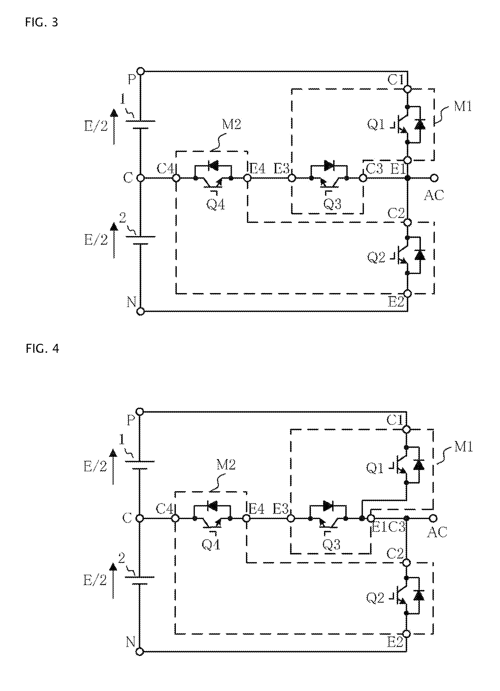
[0044]FIG. 3 is a diagram for illustrating the power converter according to the invention.

[0045]In FIG. 3, each of the semiconductor devices M1 and M2, in the same way as the semiconductor devices M1 and M2 shown in FIG. 1, has four terminals, and the configuration thereof is also the same.

[0046]Also, the first series circuit is also the same as the first series circuit shown in FIG. 1.

[0047]The second series circuit is a circuit wherein the semiconductor switching element Q3 of the semiconductor device M1 and the semiconductor switching element Q4 of the semiconductor device M2 are connected in anti-series. In order to configure the second series circuit, the terminal E3 of the semiconductor device M1 and the terminal E4 of the semiconductor device M2 are connected. By so doing, the semiconductor switching element Q3 and the semiconductor switching element Q4 are connected in anti-series. Also, the terminal C3 of the semiconductor device M1 is connected to the connection point of t...


PUM


Abstract

A power converter can be configured of a first series circuit, formed from a first semiconductor switching element and a second semiconductor switching element connected in series to either end of a direct current voltage supply series circuit formed from a first direct current voltage supply and a second direct current voltage supply connected in series, and a second series circuit, formed from a third semiconductor switching element and a fourth semiconductor switching element connected in series between a connection point of the first direct current voltage supply and the second direct current voltage supply and a connection point of the first semiconductor switching element and the second semiconductor switching element. The first semiconductor switching element and the third semiconductor switching element can be configured of a first semiconductor device, and the second semiconductor switching element and the fourth semiconductor switching element can be configured of a second semiconductor device.

Description

BACKGROUND OF THE INVENTION[0001]1. Technical Field[0002]Embodiments of the present invention relate to power converters, and, in particular, three-level power converters.[0003]2. Related Art[0004]A three-level power converter is employed in a power converter that converts direct current power to alternating current power or alternating current power to direct current power. A three-level power converter can reduce alternating current voltage waveform distortion, enabling a reduction of unwanted sound and noise.[0005]FIG. 9 shows a circuit of a three-level power converter disclosed in Japanese Patent Application No. 2002-247862. In FIG. 9, reference numeral 1 is a first direct current power supply, 2 is a second direct current power supply, M10 and M20 are semiconductor devices, and Q1 to Q4 are first to fourth semiconductor switching elements.[0006]The first direct current power supply 1 and the second direct current power supply 2 are connected in series, configuring a direct curr...

Claims


Application Information

Patent Timeline
Patent Type & Authority Applications(United States)
IPC IPC(8): H02J1/00
CPCH02M7/487H02M7/003
Inventor ABE, YASUSHIHASHII, MAKOTOTAKAHASHI, KIYOSHI
Owner FUJI ELECTRIC CO LTD
Why Eureka
Try Eureka