Light Emitting Device and Method for Manufacturing Thereof

Inactive Publication Date: 2012-10-11
SEMICON ENERGY LAB CO LTD
View PDF2 Cites 7 Cited by
  • Summary
  • Abstract
  • Description
  • Claims
  • Application Information

AI Technical Summary

Benefits of technology

[0029]According to one embodiment of the present invention, a light-emitting device in which generation of luminance unevenness due to a voltage drop and a decrease in emission luminance due to an auxiliary wiring are suppressed can be provided.
[0030]Further, according to one embodiment of the present invention, an EL layer is formed by eva

Problems solved by technology

Thus, when the second electrode is formed over a large area, luminance unevenness occurs in a light-e

Method used


Image

  • Light Emitting Device and Method for Manufacturing Thereof
  • Light Emitting Device and Method for Manufacturing Thereof
  • Light Emitting Device and Method for Manufacturing Thereof

Examples


Example

Embodiment 1

[0043]In this embodiment, a light-emitting device and a method for manufacturing the light-emitting device according to one embodiment of the disclosed invention is described with reference to FIGS. 1A to 1C, FIGS. 2A to 2D, FIG. 3, FIGS. 4A and 4B, FIGS. 5A and 5B, FIGS. 6A and 6B, and FIGS. 11A and 11B.

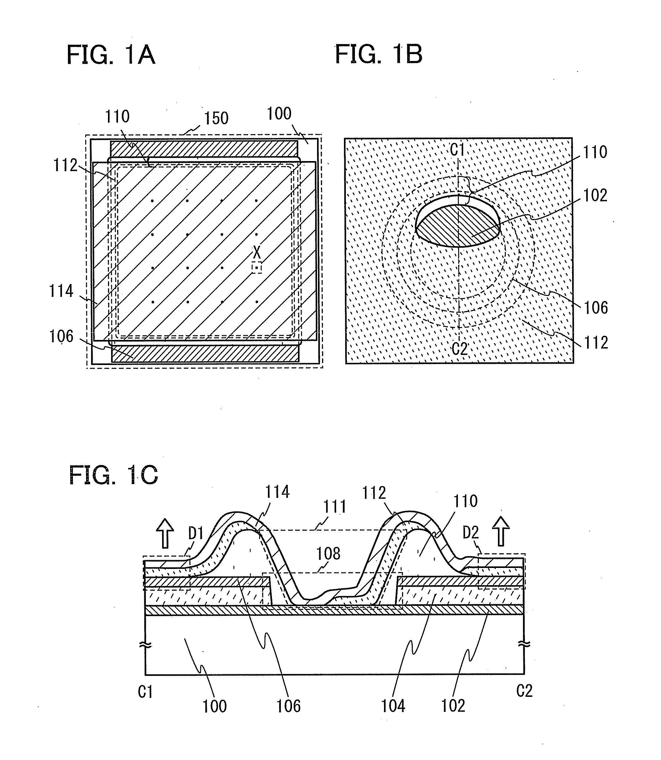
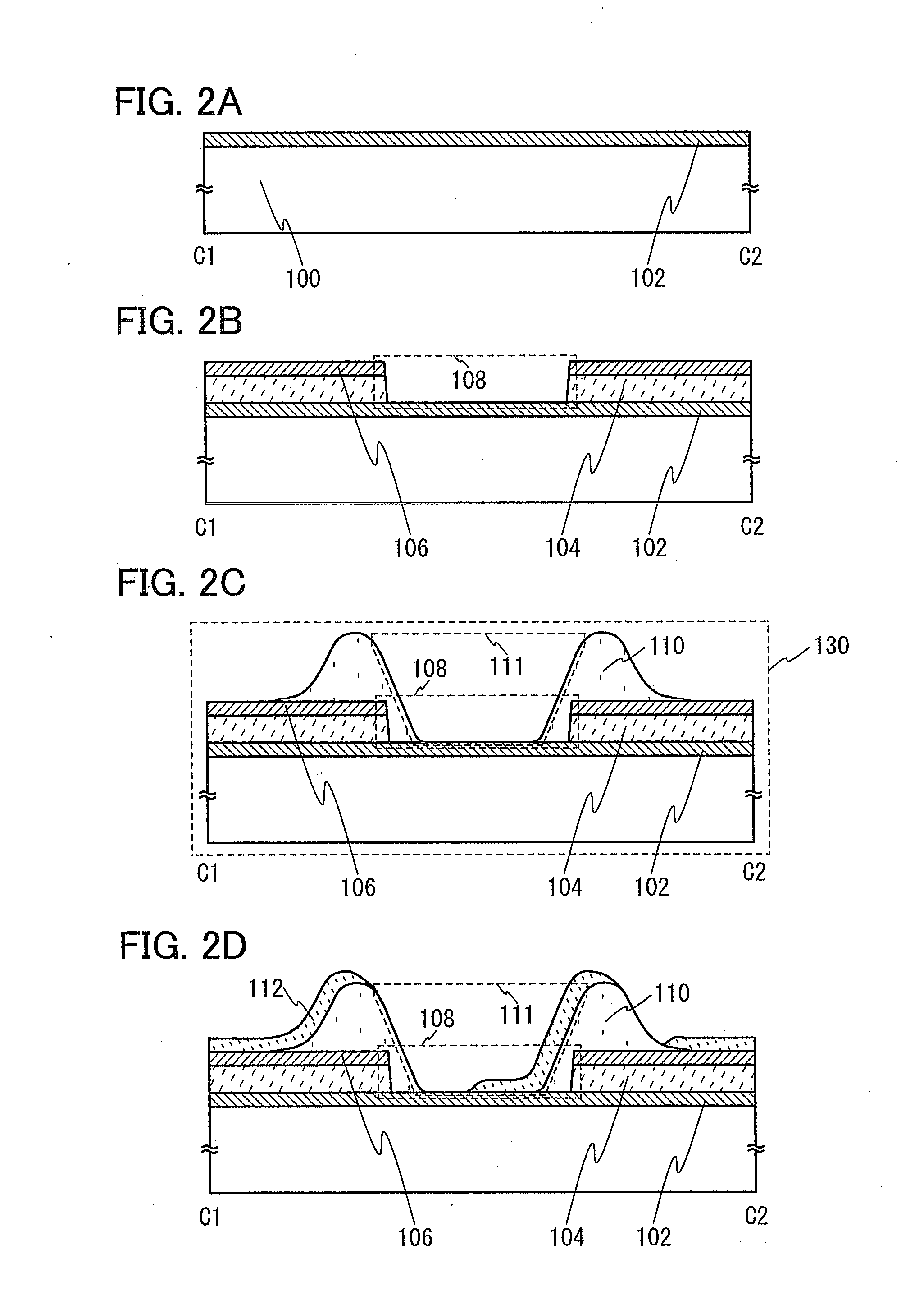
[0044]FIGS. 1A to 1C illustrate a top-emission light-emitting device that is an example of a light-emitting device of this embodiment. FIG. 1A is a top view of a light-emitting device 150 and FIG. 1B is an enlarged view of a portion X squarely surrounded by a dotted line in FIG. 1A. In FIG. 1B, some of components are omitted to avoid complexity.

[0045]FIG. 1C is a cross-sectional view of the light-emitting device 150 taken along dashed-dotted line C1-C2 in FIG. 1B.

[0046]In the top-emission light-emitting device 150 described in this embodiment, as illustrated in FIG. 1C, a conductive layer 102 serving as an auxiliary wiring is provided under a first electrode 106 serving ...

Example

Embodiment 2

[0105]In this embodiment, a light-emitting device whose structure is partially different from that of the light-emitting device manufactured in Embodiment 1 and a method for manufacturing the light-emitting device will be described with reference to FIGS. 7A to 7C and FIGS. 8A and 8B. In the structure of this embodiment described below, the same portions or portions having similar functions are denoted by the same reference numerals in different drawings, in Embodiment 1, and the description thereof is not repeated.

[0106]FIGS. 7A to 7C illustrate a top-emission light-emitting device that is an example of a light-emitting device of this embodiment. FIG. 7A is a top view of a light-emitting device 750, and FIG. 7B is an enlarged view of a portion J squarely surrounded by a dotted line in FIG. 7A. In FIG. 7B, some of components are omitted to avoid complexity.

[0107]FIG. 7C is a cross-sectional view of the light-emitting device 750 taken along dashed-dotted line G1-G2 in FIG...

Example

Embodiment 3

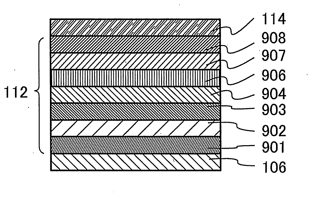
[0120]In this embodiment, an example of the EL layer 112 which can be applied to one embodiment of the present invention will be described with reference to FIGS. 9A to 9C.

[0121]As illustrated in FIG. 9A, the EL layer 112 is provided between the first electrode 106 and a second electrode 114. The first electrode 106 and the second electrode 114 can have structures similar to those in the above embodiments.

[0122]The EL layer 112 includes at least a light-emitting layer containing a light-emitting organic compound. In addition, the EL layer 112 can have a stacked-layer structure in which a layer containing a substance having a high electron-transport property, a layer containing a substance having a high hole-transport property, a layer containing a substance having a high electron-injection property, a layer containing a substance having a high hole-injection property, a layer containing a bipolar substance (a substance having a high electron-transport property and a high...


PUM


Abstract

A conductive layer serving as an auxiliary wiring is formed under a first electrode with a first insulating layer interposed therebetween, and the conductive layer and a second electrode are electrically connected to each other through an opening in the first insulating layer and the first electrode. A second insulating layer is formed over a sidewall of the opening so that the first electrode is not directly in contact with the second electrode in the opening. An EL layer is formed by evaporation in a state where a deposition target substrate is inclined to an evaporation source, so that the second insulating layer serves as an obstacle and a region where the EL layer is not formed by the evaporation and the conductive layer is exposed is formed in part of the opening in a self-aligned manner.

Description

BACKGROUND OF THE INVENTION[0001]1. Field of the Invention[0002]The present invention relates to a light-emitting device and a method for manufacturing thereof.[0003]2. Description of the Related Art[0004]Instead of light-emitting devices such as incandescent lamps and fluorescent lamps which have been used for a long time, in recent years, a light-emitting device using an element (hereinafter, abbreviated to an EL element) in which a functional thin film layer (hereinafter, abbreviated to an EL (Electro Luminescence) layer) which emits light by application of current is interposed between electrodes has been actively researched. A light-emitting device including an EL element has advantages that reduction in thickness and weight is easily conducted as compared to conventional light-emitting devices. The light-emitting device can be attached on a curved surface utilizing these advantages.[0005]An example of a structure of the light-emitting device including an EL element is a top em...

Claims


Application Information

Patent Timeline
IPC IPC(8): H01L51/52H01L51/56
CPCH10K50/824H10K2102/3026
Inventor TSURUME, TAKUYAIKEDA, HISAO
Owner SEMICON ENERGY LAB CO LTD
Why Eureka
Try Eureka