Apparatuses, systems and methods for treating substrate

a technology of apparatus and substrate, applied in the direction of cleaning using tools, chemistry apparatus and processes, coatings, etc., can solve the problems of increasing the number of semiconductor devices and complicated process of fabricating semiconductor devices, and achieve the effect of minimizing the unnecessary carrying of substrates

Active Publication Date: 2013-01-31
SEMES CO LTD
View PDF4 Cites 126 Cited by
  • Summary
  • Abstract
  • Description
  • Claims
  • Application Information

AI Technical Summary

Benefits of technology

[0006]The present invention provides an apparatus, system and method for treating a substrate, which minimizes unnecessary carrying of a substrate.

Problems solved by technology

As semiconductor devices are miniaturized, processes of fabricating a semiconductor device become complicated, and the number thereof is increased.

Method used


Image

  • Apparatuses, systems and methods for treating substrate
  • Apparatuses, systems and methods for treating substrate
  • Apparatuses, systems and methods for treating substrate

Examples


Embodiment Construction

[0046]The terms and accompanying drawings used herein are exemplary terms and drawings for describing exemplary embodiments of the present invention, and thus, the present invention is not limited thereto.

[0047]Moreover, detailed descriptions related to well-known technologies will be ruled out in order not to unnecessarily obscure subject matters of the present invention.

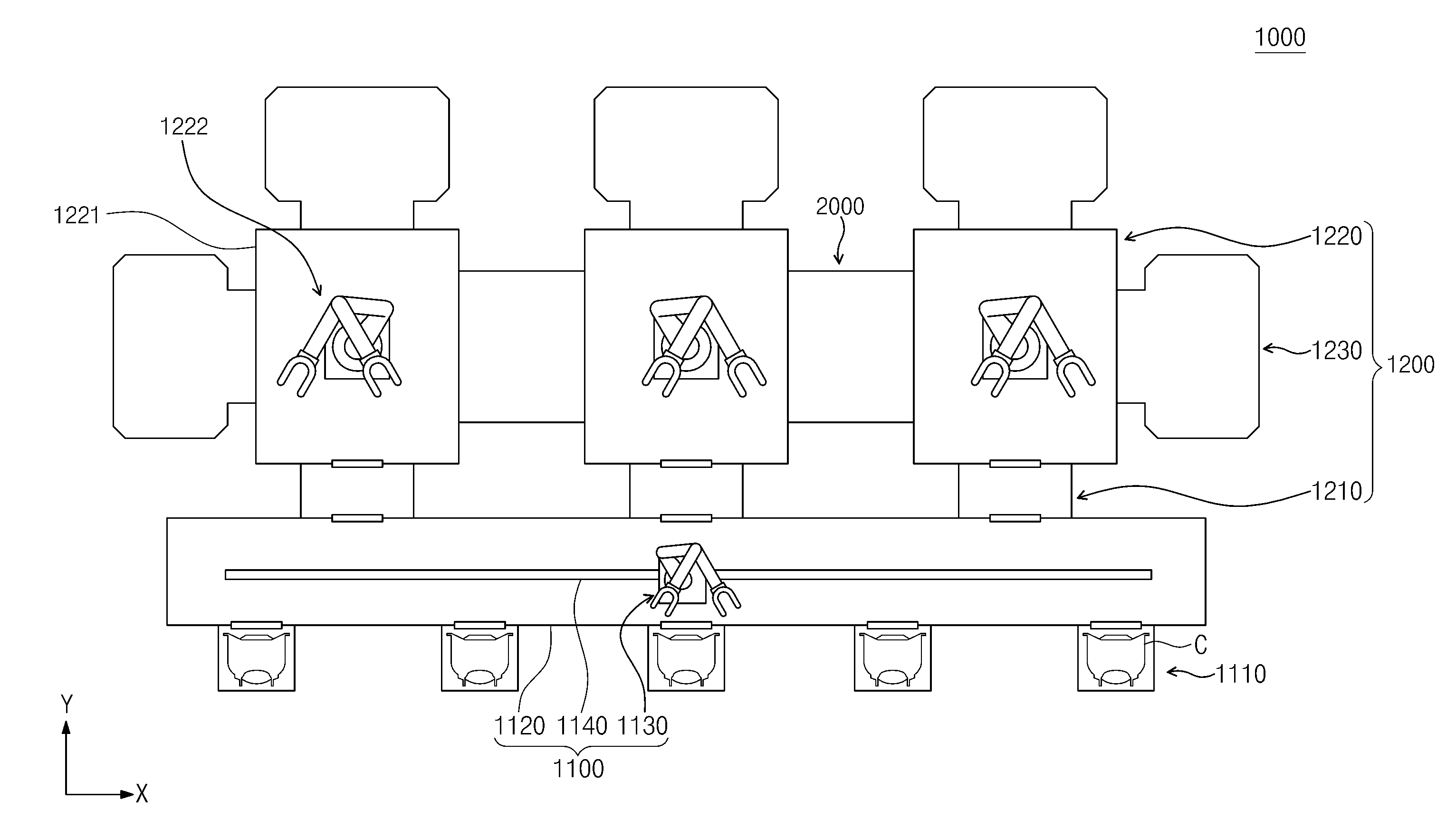
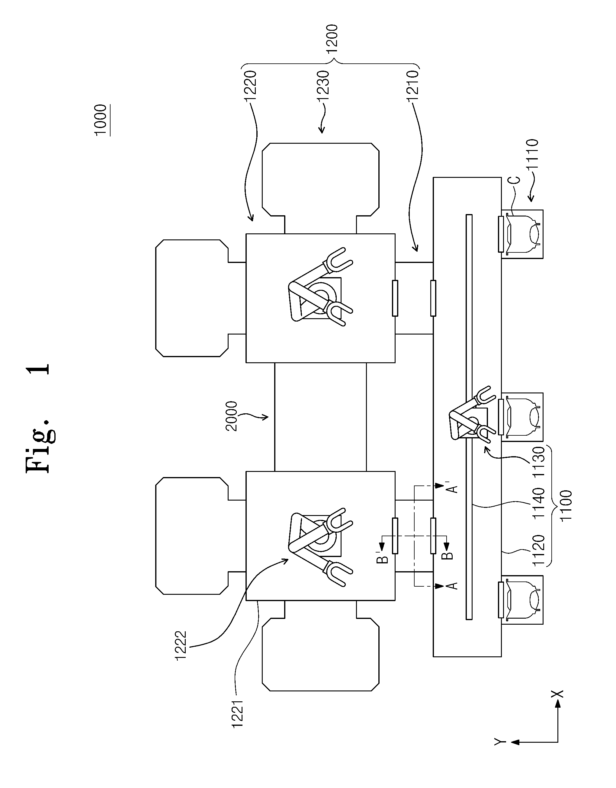
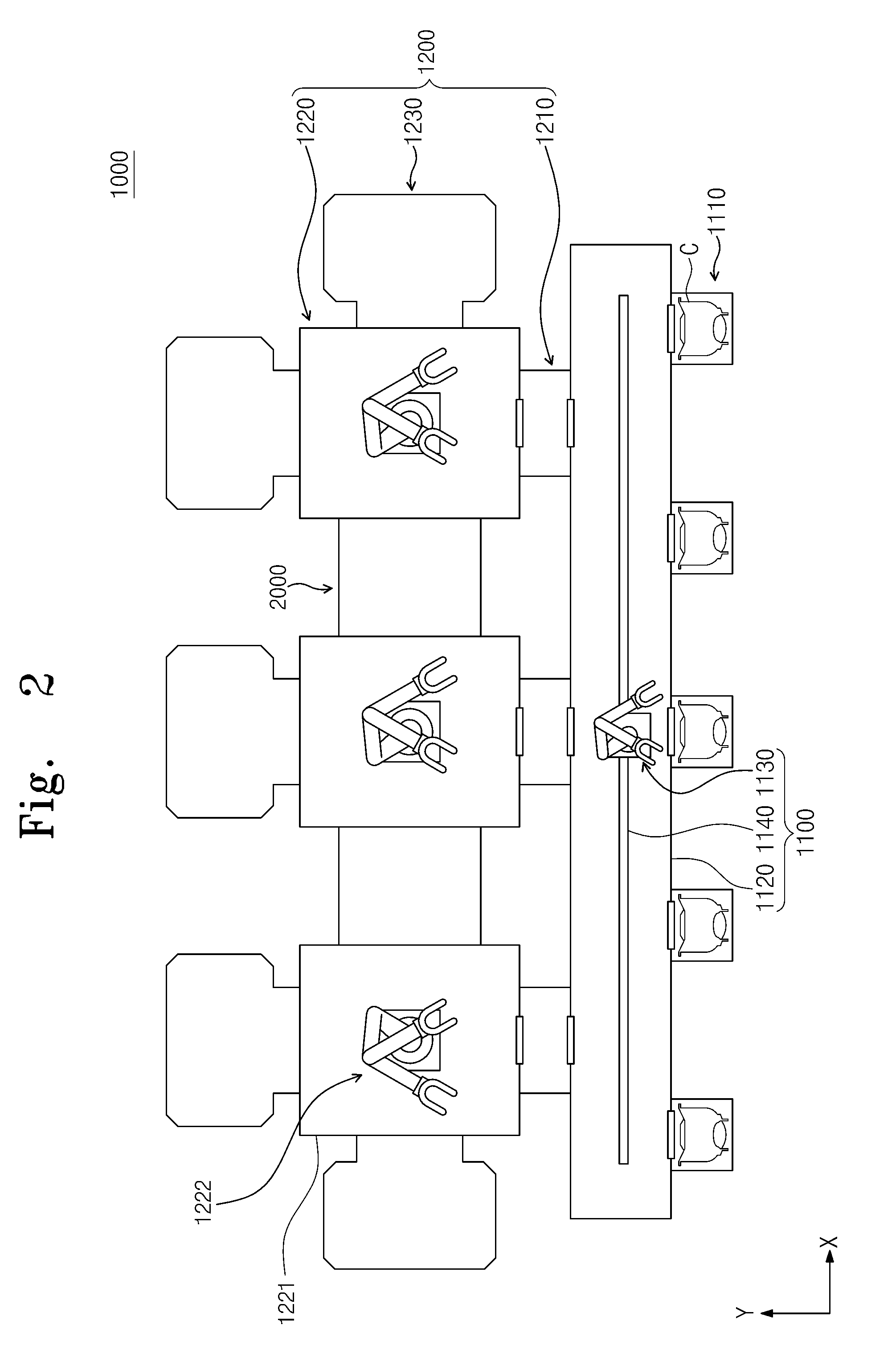
[0048]Hereinafter, a substrate treating apparatus 1000 according to an embodiment of the present invention will now be described.

[0049]The substrate treating apparatus 1000 may perform a process on a substrate S. The process may be any process used to fabricate a semiconductor device, a flat panel display (FPD), and a device including a circuit on a thin film. In addition, the substrate S may be any substrate used to fabricate a semiconductor device, an FPD, and a device including a circuit on a thin film. For example, the substrate S may be a silicon wafer or one of various wafers, organic substrates, and glass su...


PUM

PropertyMeasurementUnit
cluster structureaaaaaaaaaa
plasmaaaaaaaaaaa
shapeaaaaaaaaaa

Abstract

Provided is an apparatus, system and method for treating a substrate, and more particularly, a substrate treating apparatus having a cluster structure, a substrate treating system, and a substrate treating method using the substrate treating system. The substrate treating apparatus includes a load port on which a container containing a substrate is installed, a plurality of process modules treating the substrate, a transfer module disposed between the load port and the process modules, and transferring the substrate between the container and the process modules, and a buffer chamber disposed between neighboring ones of the process modules, and providing a space for carrying the substrate between the neighboring process modules.

Description

CROSS-REFERENCE TO RELATED APPLICATIONS[0001]This U.S. non-provisional patent application claims priority under 35 U.S.C. §119 of Korean Patent Application Nos. 10-2011-0076208, filed on Jul. 29, 2011, and 10-2011-0128270, filed on Dec. 2, 2011, the entire contents of which are hereby incorporated by reference.BACKGROUND OF THE INVENTION[0002]The present invention disclosed herein relates to an apparatus, system and method for treating a substrate, and more particularly, to a substrate treating apparatus having a cluster structure, a substrate treating system, and a substrate treating method using the substrate treating system.[0003]Semiconductor devices may be fabricated by forming circuit patterns on a substrate such as a silicon wafer through various multi-stage processes including photolithography. Such multi-stage processes are performed in corresponding chambers. Thus, an operation that a substrate is put in a chamber for performing a process, and is then put in another chambe...

Claims


Application Information

Patent Timeline
Patent Type & Authority Applications(United States)
IPC IPC(8): B05C13/02B08B7/00B44C1/22B32B38/10C23C16/50C23C16/458
CPCH01L21/67109H01L21/67167Y10T156/19H01L21/67196Y10T156/11H01L21/67184
Inventor KIM, HYUNG JOON
Owner SEMES CO LTD
Why Eureka
Try Eureka