This helps you quickly interpret patents by identifying the three key elements:
Problems solved by technology
Method used
Benefits of technology
Benefits of technology
[0039]In a semiconductor light-emitting element according to the present invention, a striped structure that runs in a direction that defines an angle of either 5 degrees or more or −5 degrees or less with respect to the a-axis is provided for the light-emitting face through which the light emitted from the active layer region is extracted. Thus, polarized light can be incident as a composite wave of p- and s-waves on the slope of projections that form the striped structure. The light that has been incident as such a composite wave of p- and s-waves has its polarization direction changed and is transmitted. Also, the percentage of the p- and s-waves of the light that has been incident on the slope can be varied in a wide range by the striped structure. As a resul
Problems solved by technology
Consequently, due to the quantum confinement Stark effect of carriers, the internal quantum efficiency of the active layer decreases, thus increasing the threshold current in a semiconductor laser diode and increasing the power dissipation and decreasing the luminous efficacy in an LED.
However, if a
Method used
Image
Click on the blue label to locate the original text in one second.
Reading with bidirectional positioning of images and text.
Examples
Example
Making Example 1, Reference Example 1 and Comparative Example 1
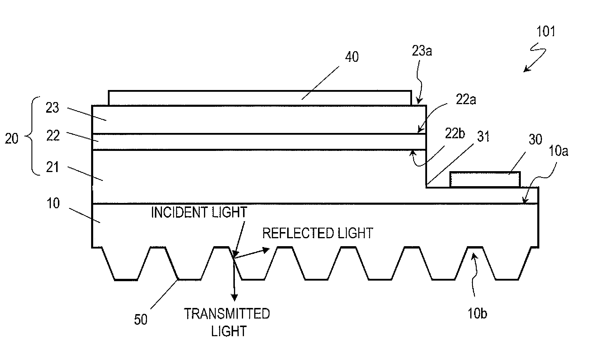
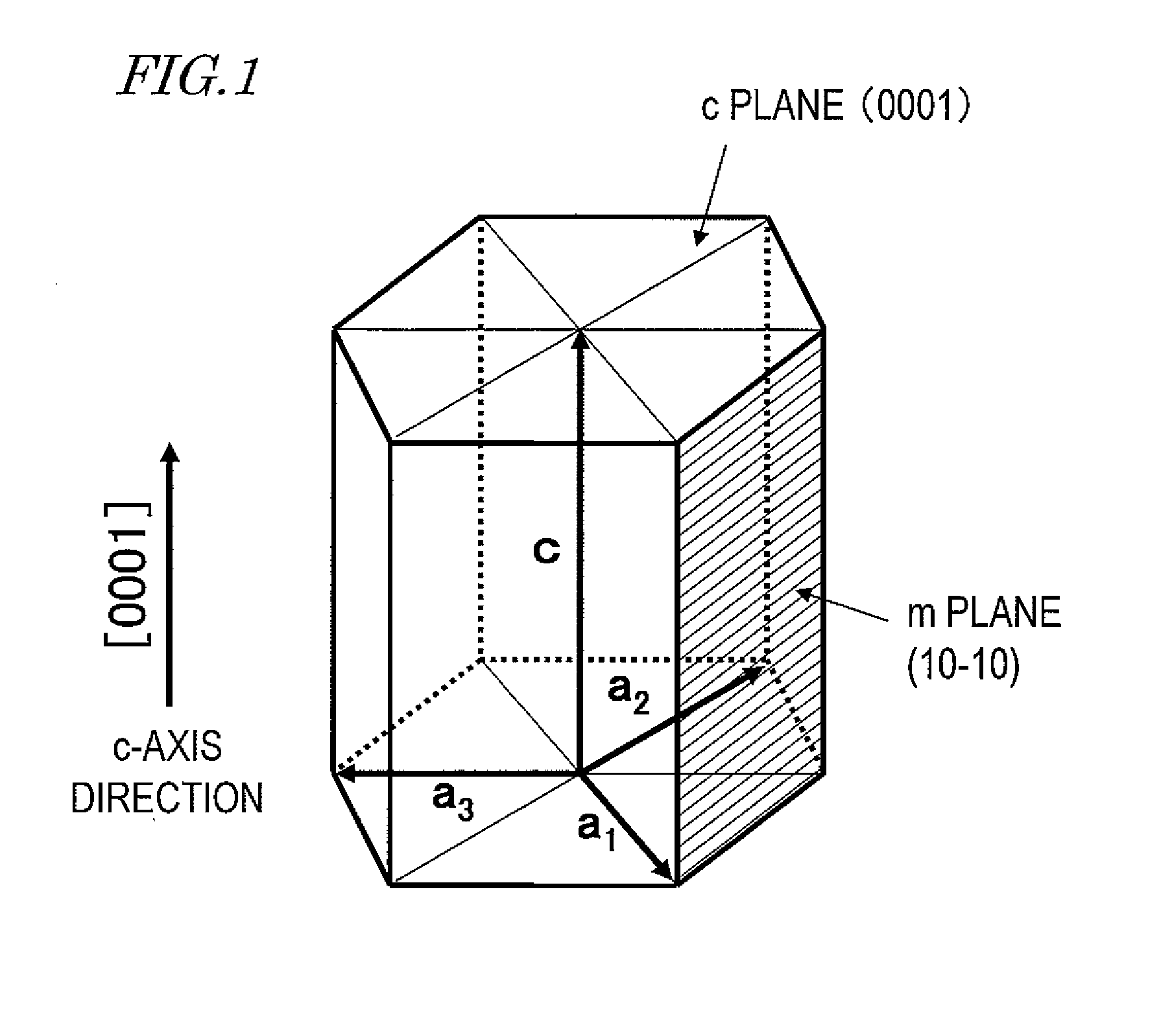
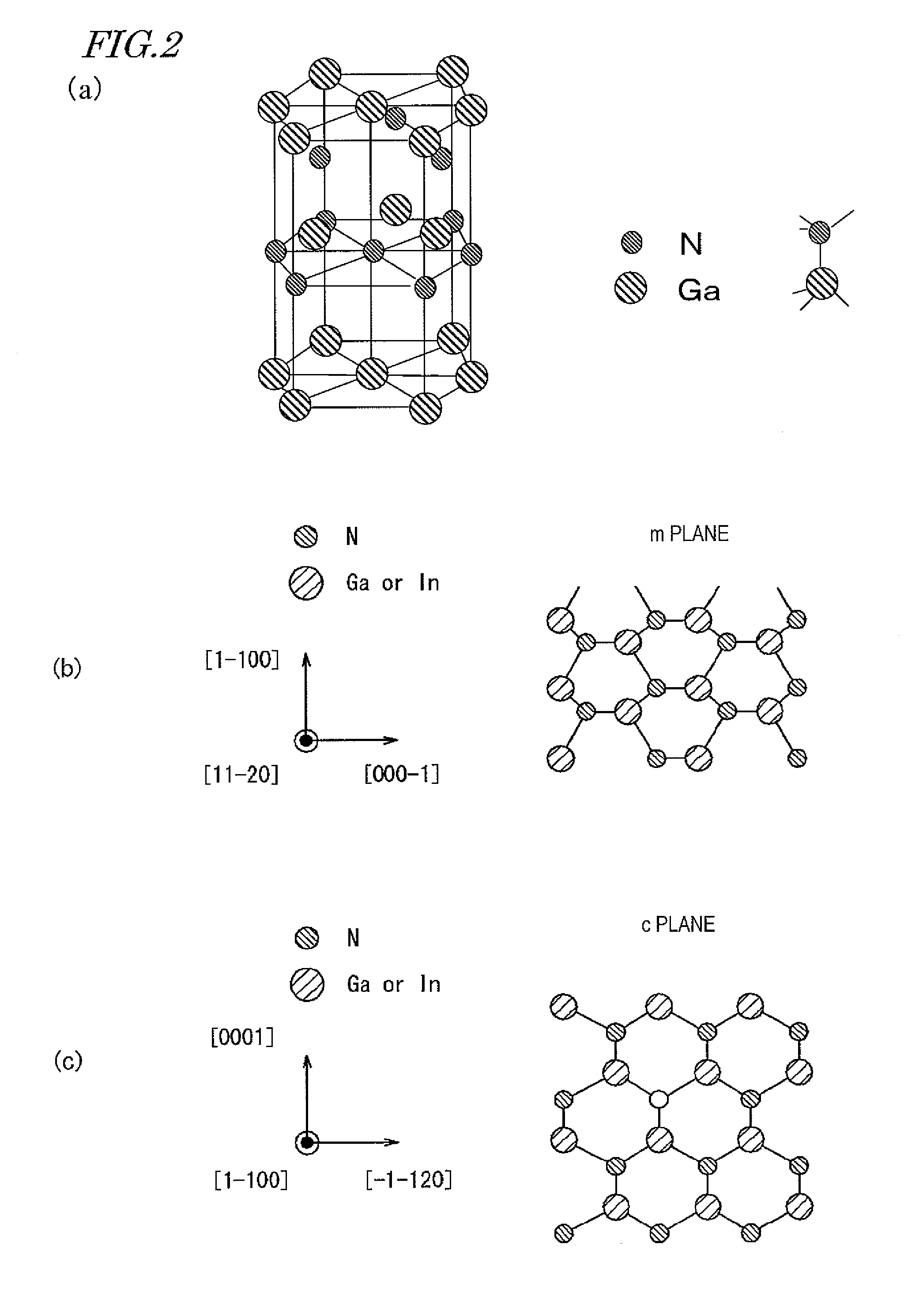
[0167]First of all, as shown in FIG. 3, a semiconductor multilayer structure 20 was grown epitaxially on a substrate 10 by MOCVD (metalorganic chemical vapor deposition) process. Specifically, an n-type nitride semiconductor layer 21 was grown epitaxially on an n-type GaN substrate, of which the principal surface was an m plane. For example, using silicon as an n-type dopant and supplying TMG (Ga(CH3)3) and NH3 as source gases to a reaction chamber, an n-type nitride semiconductor layer 21 of GaN was deposited to a thickness of 3 μm at a growing temperature of approximately 1050 degrees Celsius.
[0168]Next, an active layer region 22 was formed on the n-type nitride semiconductor layer 21. The active layer region 22 had a GaInN / GaN multiple quantum well (MQW) structure in which Ga1-xInxN well layers (where x=0.19), each having a thickness of 9 nm, and GaN barrier layers, each having a thickness of 9 nm, were stacked altern...
Example
Making Example 2, Reference Example 2 and Comparative Example 2
[0176]A portion functioning as a semiconductor light-emitting element was made in the same procedure as in Example 1, Reference Example 1 and Comparative Example 1. After that, a striped structure was made in a different procedure from in Example 1, Reference Example 1 and Comparative Example 1. Specifically, an SiO2 film was deposited as a hard mask material on the second principal surface 10b of the substrate 10. The SiO2 film was deposited by plasma chemical vapor deposition process. Next, a photoresist was applied onto the hard mask and was patterned using a contact exposure system. Thereafter, using the photoresist as a mask, the hard mask was dry-etched with CF4 gas and O2 gas. Next, using the hard mask as a mask, the second principal surface 10b of the substrate 10 was dry-etched using a chlorine based gas. Finally, the hard mask was removed by dry etching. In this manner, a semiconductor light-emitting element wa...
Example
Making Example 3, Reference Example 3 and Comparative Example 3
[0178]Semiconductor light-emitting elements, of which the striped structure defined angles β of 0, 5, 30, 45 and 90 degrees, respectively, with respect to the a-axis, were fabricated. First of all, a portion functioning as a semiconductor light-emitting element was made in the same procedure as in Example 1, Reference Example 1 and Comparative Example 1. After that, a striped structure was made in a different procedure from in Example 1, Reference Example 1 and Comparative Example 1. Specifically, a photoresist was applied onto the second principal surface 10b of the substrate 10 and was patterned using a contact exposure system and then heated to 230 degrees Celsius. Thereafter, using the photoresist as a mask, the second principal surface 10b of the substrate 10 was dry-etched using a chlorine based gas. In this process step, the photoresist was also removed at the same time as a result of the dry etching process. In t...
PUM
Abstract
A semiconductor light-emitting element according to the present invention includes: an n-type nitride semiconductor layer 21; a p-type nitride semiconductor layer 23; an active layer region 22 which includes an m-plane nitride semiconductor layer and which is interposed between the n- and p-type nitride semiconductor layers; an n-type electrode 30 which is electrically connected to the n-type nitride semiconductor layer; a p-type electrode 40 which is electrically connected to the p-type nitride semiconductor layer; a light-emitting face, through which polarized light that has been produced in the active layer region is extracted out of this element; and a striped structure 50 which is provided for the light-emitting face and which has a plurality of projections that run in a direction that defines either an angle of 5 degrees to 80 degrees or an angle of −80 degrees to −5 degrees with respect to the a-axis direction of the m-plane nitride semiconductor layer.
Description
TECHNICAL FIELD[0001]The present invention relates to a nitride-based semiconductor light-emitting element and more particularly relates to a semiconductor light-emitting element, of which the principal surface is an m plane.BACKGROUND ART[0002]A nitride semiconductor including nitrogen (N) as a Group V element is a prime candidate for a material to make a short-wave light-emitting element because its bandgap is sufficiently wide. Among other things, gallium nitride-based compound semiconductors have been researched and developed particularly extensively. As a result, blue-ray-emitting light-emitting diodes (LEDs), green-ray-emitting LEDs and semiconductor laser diodes made of gallium nitride based semiconductors have already been used in actual products (see Patent Documents Nos. 1 and 2).[0003]In the following description, gallium nitride based compound semiconductors will be referred to herein as “nitride-based semiconductors”. Nitride-based semiconductors include compound semico...
Claims
Application Information
Patent Timeline
Application Date:The date an application was filed.
Publication Date:The date a patent or application was officially published.
First Publication Date:The earliest publication date of a patent with the same application number.
Issue Date:Publication date of the patent grant document.
PCT Entry Date:The Entry date of PCT National Phase.
Estimated Expiry Date:The statutory expiry date of a patent right according to the Patent Law, and it is the longest term of protection that the patent right can achieve without the termination of the patent right due to other reasons(Term extension factor has been taken into account ).
Invalid Date:Actual expiry date is based on effective date or publication date of legal transaction data of invalid patent.

