

LED package structure and manufacturing method for the same
- Summary
- Abstract
- Description
- Claims
- Application Information
AI Technical Summary
Benefits of technology
Problems solved by technology
Method used
Image

Examples
Embodiment Construction
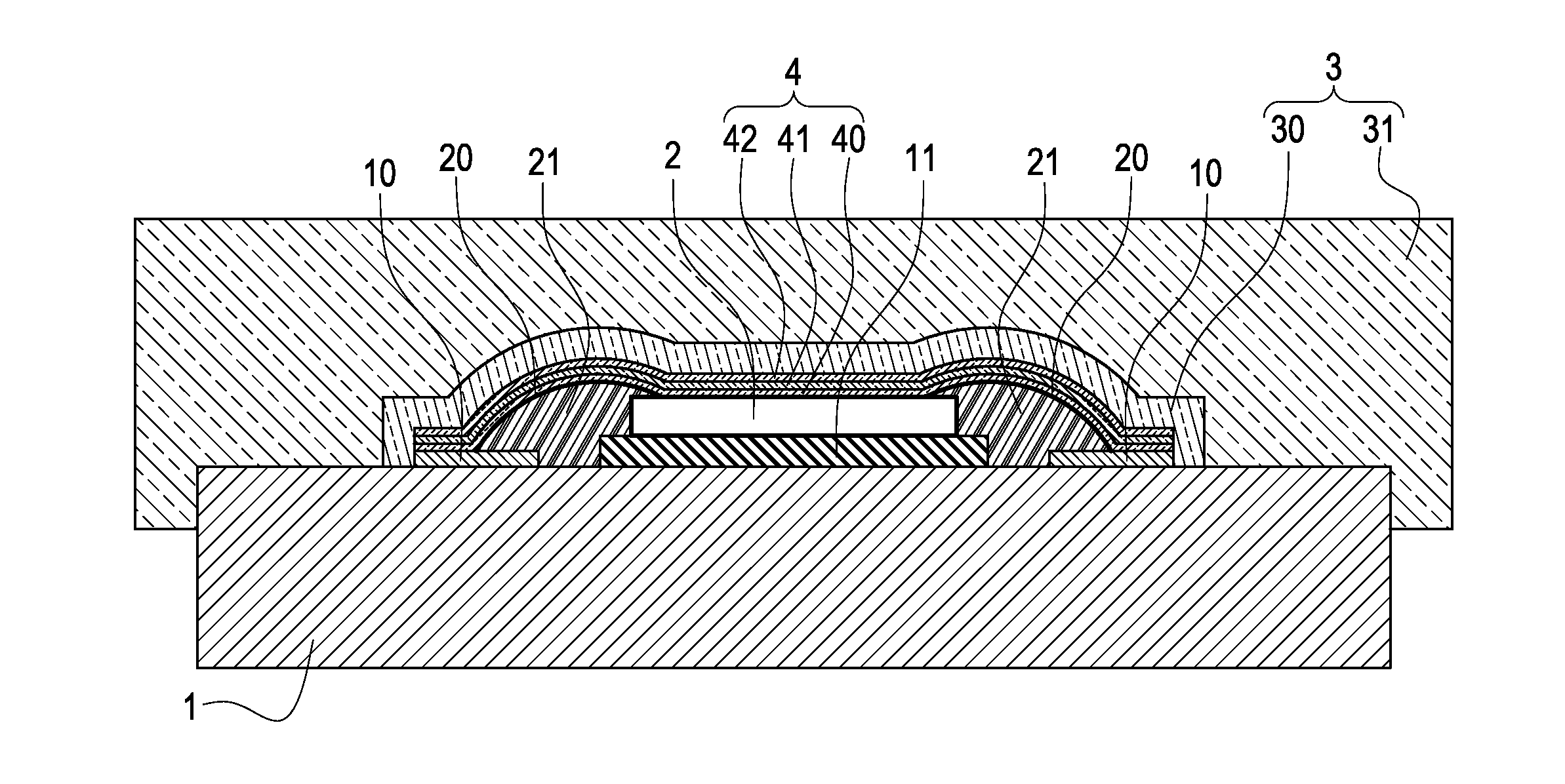
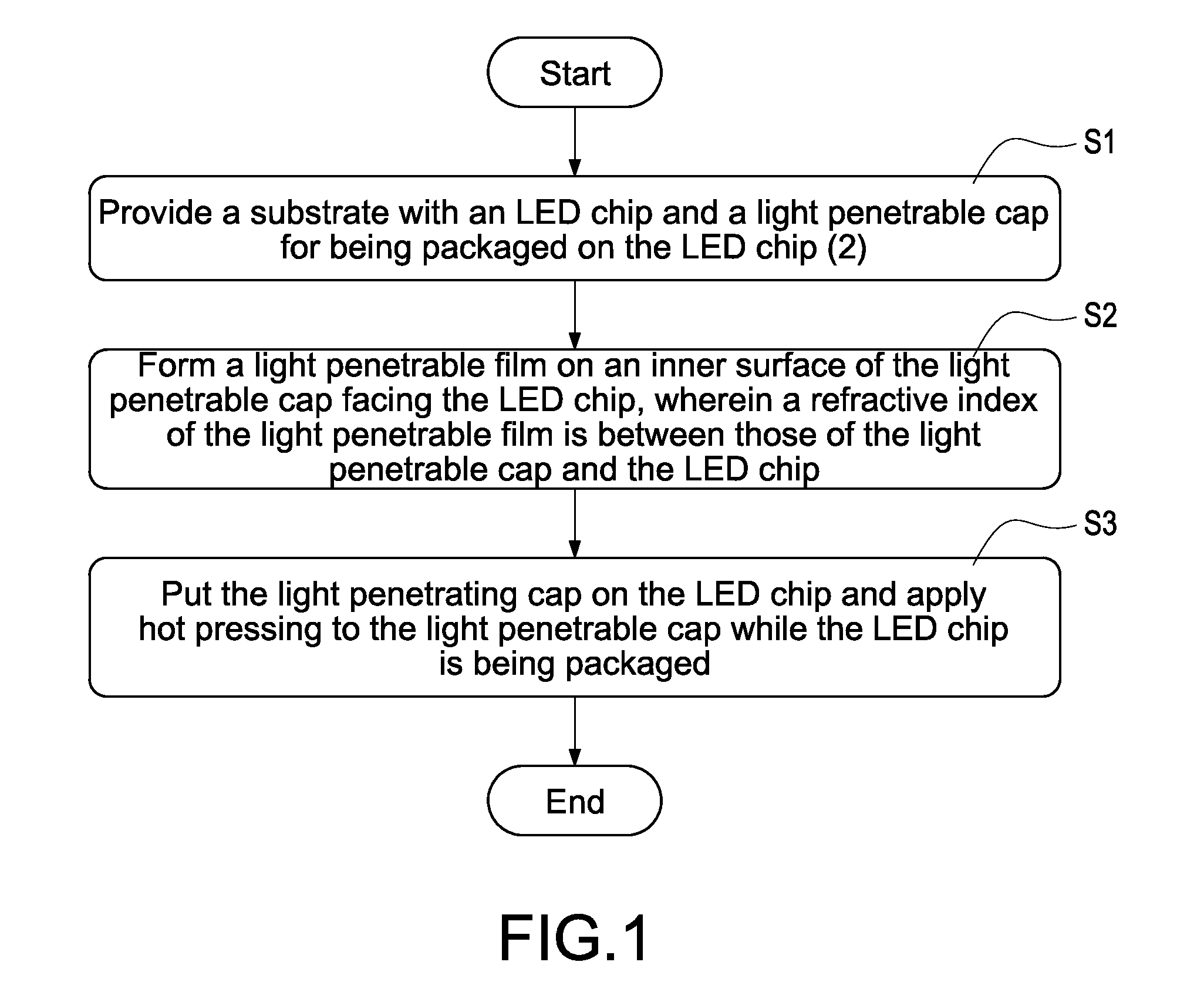
[0018]The invention provides an LED package structure and a manufacture method for the same. The invention adds at least one light penetrable film, whose refractive index is between the LED chip and the lens, in the lens of the LED chip. Thereby the light extraction efficiency can be increased.
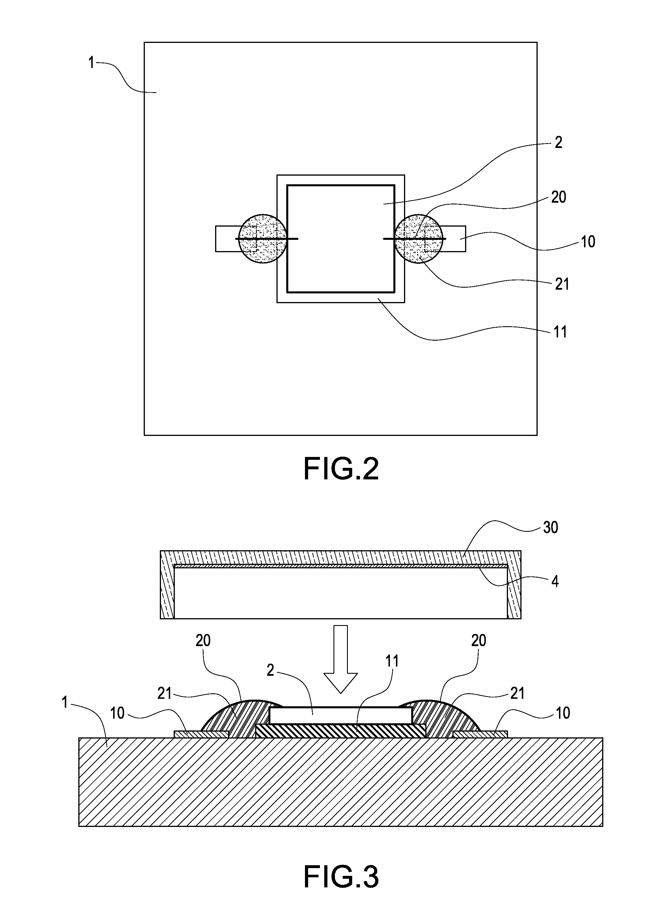
[0019]FIG. 1 is a flowchart of the method of the invention. Please refer to FIGS. 1-3. In step S1, a substrate 1 with an LED chip 2 and a light penetrable cap 30 for being packaged on the LED chip 2 are provided. As shown in FIG. 2, the substrate 1 with LED chip 2 is provided with two conductive layers 10 as a positive electrode and a negative electrode. The LED chip 2 is located between the two conductive layers 10 and is separately electrically connected to the two conductive layers 10 by two wires 20. The wires 20 are applied with an adhesive 21 such as silicone for fixation to prevent the wires 20 from being broken. Additionally, silver epoxy may be applied between the LED chip 2 and the s...
PUM
 Abstract
Description
Claims
Application Information