Liquid crystal display device

a display device and liquid crystal technology, applied in non-linear optics, instruments, optics, etc., can solve the problems of black transmittance increasing and white transmittance decreasing, and achieve the effect of increasing black transmittance, white transmittance decreasing, and improving display mode efficiency

Active Publication Date: 2013-06-13
JAPAN DISPLAY INC
View PDF7 Cites 18 Cited by
  • Summary
  • Abstract
  • Description
  • Claims
  • Application Information

AI Technical Summary

Benefits of technology

[0010]The present invention is provided in view of these problems, and an object of the present invention is to provide a liquid crystal display device where the display mode efficiency can be increased by making the distribution of the electrical field uniform within pixels.
[0019]According to the present invention, the distribution of the electrical field can be made uniform within the pixels, and thus, the display mode efficiency can be increased.

Problems solved by technology

As a result, liquid crystal moves due to the effects of a potential around pixels, for example, a potential in a signal wire, such as a gate line or a drain line, and a potential in an adjacent pixel, and such a problem arises that the transmittance of black increases.
In addition, in the case where an electrode that forms a capacitor (hereinafter referred to as capacitor electrode) is provided in a layer beneath a wall electrode, such a problem arises that the potential in the capacitor electrode, the potential in a signal wire and the potential around the pixel, that is the potential in an adjacent pixel, have such an effect that the transmittance of white lowers.

Method used


Image

  • Liquid crystal display device
  • Liquid crystal display device
  • Liquid crystal display device

Examples


first embodiment

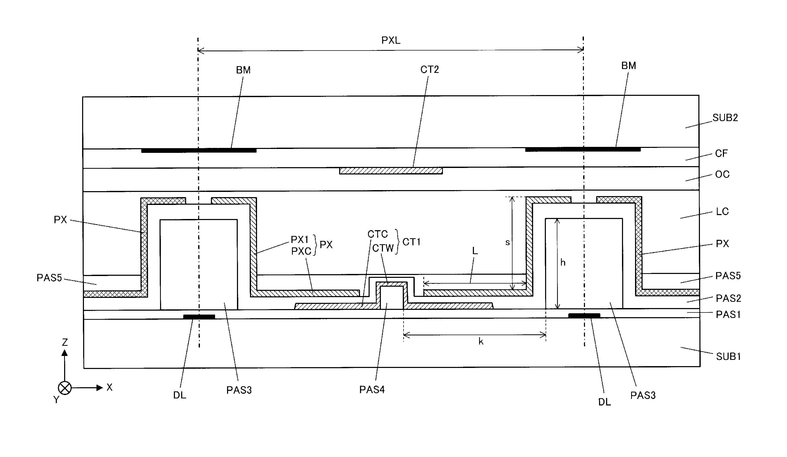
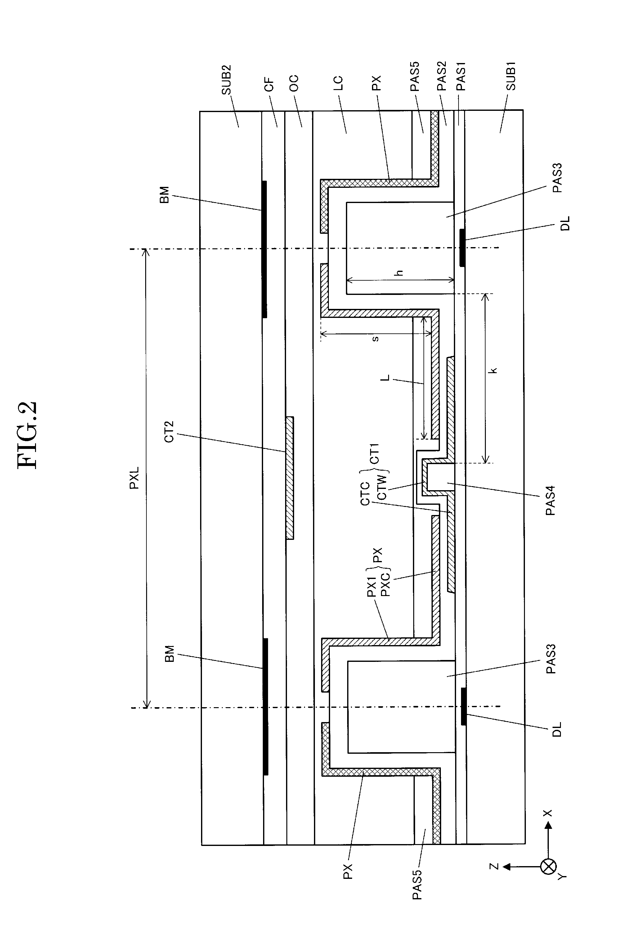
[0042]FIG. 1 is a plan diagram for illustrating the entirety of the structure of a liquid crystal display device according to the first embodiment of the present invention. In the following, the entirety of the structure of the liquid crystal display device according to the first embodiment is described in reference to FIG. 1. Here, in the present specification, the transmittance gained by excluding the effects from the absorption by the color filters CF and the polarizing plates as well as the effects of the aperture ratio is referred to as display mode efficiency. Accordingly, the display mode efficiency is 100% when the linearly polarized light that has been emitted from the polarizing plate on the backlight unit side enters into the polarizing plate on the display surface side with the direction of vibration rotated by 90 degrees.

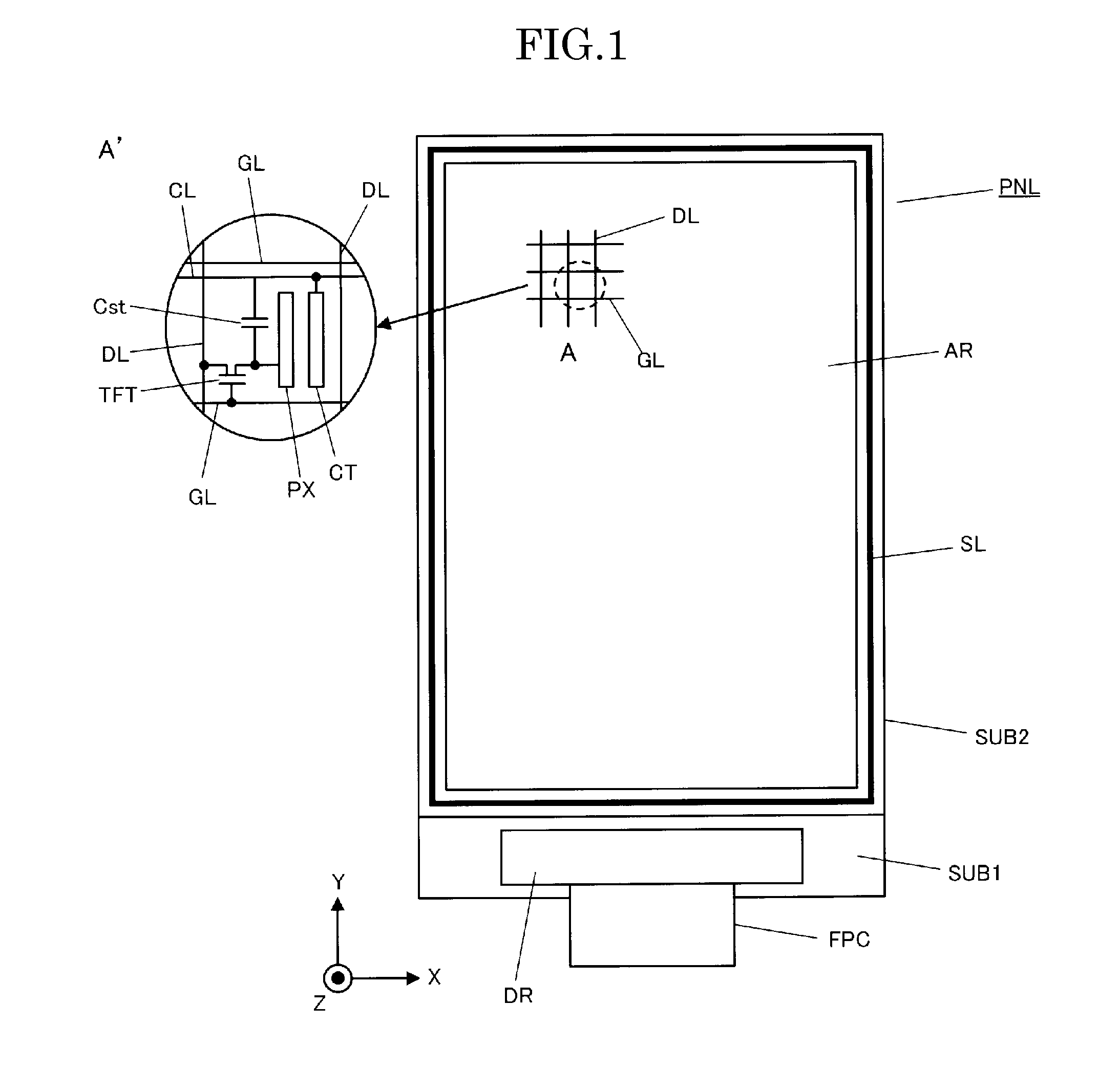
[0043]As shown in FIG. 1, the liquid crystal display device according to the first embodiment has a liquid crystal display panel PNL formed of a first ...

second embodiment

[0094]FIG. 9 is a cross-sectional diagram for schematically illustrating the structure of a liquid crystal display device according to the second embodiment of the present invention. The cross-sectional diagram in FIG. 9 corresponds to the cross-sectional diagram in FIG. 2 showing the first embodiment. Here, the liquid crystal display device according to the second embodiment has the same structure as in the first embodiment, except that the location in which the capacitor Cst is formed is different. Accordingly, in the following, a pair of electrodes that form the capacitor Cst is described in detail.

[0095]As shown in FIG. 9, the pixel structure in the liquid crystal display device according to the second embodiment has an electrode (second wall electrode) CT5 formed on a wall electrode insulating film PAS3 in pillar form on which the wall pixel electrode PX is formed, and thus, the capacitor Cst is formed.

[0096]That is to say, the common electrode CT1 for forming the pseudo-wall e...

third embodiment

[0103]FIG. 11 is a cross-sectional diagram for illustrating the pixel structure in a liquid crystal display device according to the third embodiment of the present invention, and the cross-sectional diagram in FIG. 11 corresponds to the cross-sectional diagram in FIG. 2 showing the first embodiment. Here, the liquid crystal display device according to the third embodiment has the same structure as in the first embodiment, except only that the location in which one of the electrodes for forming the capacitor Cst is formed is different. Accordingly, in the following, the pair of electrodes for forming the capacitor Cst is described in detail.

[0104]As shown in FIG. 10, in the pixel structure according to the third embodiment, the electrode CTE for forming the capacitor Cst is formed in the region through which backlight transmits and in the region where the wall pixel electrode PX is formed, and thus, the capacitor Cst is formed.

[0105]That is to say, the conductive film (transparent co...


PUM

PropertyMeasurementUnit
widthaaaaaaaaaa
voltageaaaaaaaaaa
thicknessaaaaaaaaaa

Abstract

The liquid crystal display device is provided with: a pair of first electrodes in wall form that at least partially overlap a pair of first structures; and a second electrode sandwiched between the pair of first electrodes, wherein the first electrodes are formed of: a wall electrode that is formed on a sidewall surface of the structure, protruding so as to be in a wall form in a direction of a normal to the first substrate and running in the longitudinal direction of the pixel; and a plane electrode that runs in a plane direction of the first substrate from a side of the wall electrode on the first substrate side in such a manner that an end portion thereof runs in proximity to the second electrode, and at least either the plane electrode or the second electrode covers the pixel display region.

Description

CROSS-REFERENCE TO RELATED APPLICATION[0001]The present application claims priority over Japanese Patent Application JP 2011-272343 filed on Dec. 13, 2011, the contents of which are hereby incorporated into this application by reference.BACKGROUND OF THE INVENTION[0002](1) Field of the Invention[0003]The present invention relates to a liquid crystal display device, and in particular, to an IPS type liquid crystal display device where an electrical field is applied parallel to the surfaces of the substrates.[0004](2) Description of the Related Art[0005]Liquid crystal display devices which are referred to as an IPS (in-plane switching) type are liquid crystal display devices where liquid crystal molecules are aligned horizontally to the surface of the panel and are rotated by 90 degrees within the horizontal surface when an electrical field (lateral electrical field) parallel to the panel surface is applied. In this IPS type liquid crystal display device, common electrodes are formed ...

Claims


Application Information

Patent Timeline
Patent Type & Authority Applications(United States)
IPC IPC(8): G02F1/1343
CPCG02F1/1343G02F2201/123G02F1/134363
Inventor HIRATSUKA, TAKATOITOU, OSAMU
Owner JAPAN DISPLAY INC
Why Eureka
Try Eureka