
Capacitive pressure sensing semiconductor device

a semiconductor device and capacitive pressure technology, applied in the direction of fluid pressure measurement, fluid pressure measurement by electric/magnetic elements, instruments, etc., can solve the problem of rather complicated structure of position indicators

Active Publication Date: 2013-08-01
WACOM CO LTD
View PDF5 Cites 34 Cited by
  • Summary
  • Abstract
  • Description
  • Claims
  • Application Information

AI Technical Summary

Benefits of technology

The invention provides a sealed semiconductor device that can detect pressure and is resistant to external shocks. This makes it a reliable and efficient tool for measuring pressure.

Problems solved by technology

Thus, structure of the position indicator is rather complicated.

Method used


Image

  • Capacitive pressure sensing semiconductor device
  • Capacitive pressure sensing semiconductor device
  • Capacitive pressure sensing semiconductor device

Examples


first embodiment

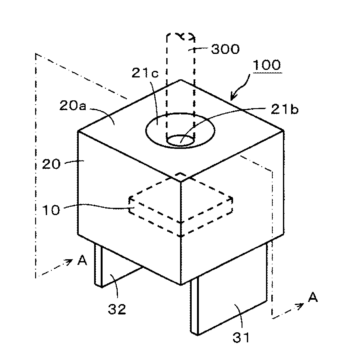
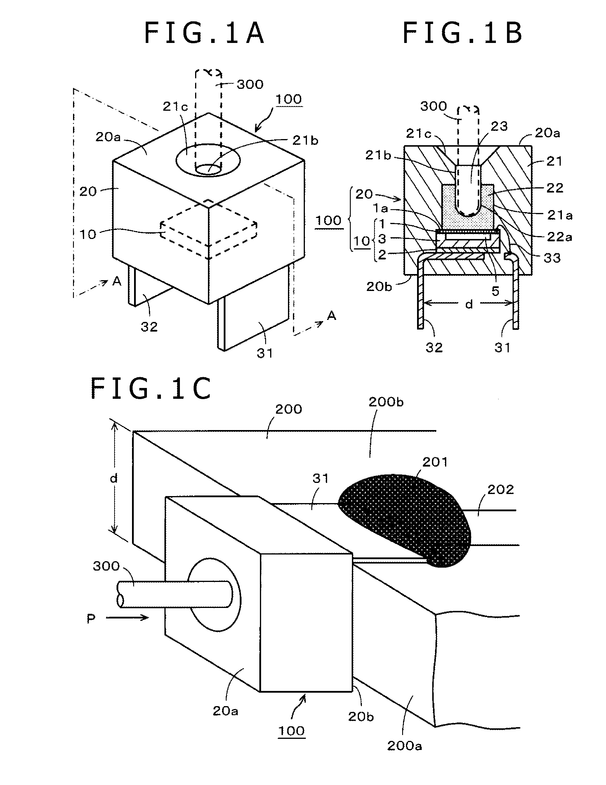
[0045]FIGS. 1A to 1C are diagrams for explaining the configuration of a first embodiment of a capacitive pressure sensing semiconductor device (hereinafter, referred to as the pressure sensing semiconductor device) according to the invention. FIG. 1A is a perspective view of a pressure sensing semiconductor device 100 of the first embodiment. FIG. 1B is a longitudinal sectional view including line A-A in FIG. 1A. FIG. 1C is a diagram showing the state when the pressure sensing semiconductor device 100 of the first embodiment is attached to a printed wiring board 200.

[0046]In the pressure sensing semiconductor device 100 of the first embodiment, a pressure detecting chip 10 configured as a semiconductor chip fabricated by a MEMS technique, for example, is sealed in a package 20 having a cubic or rectangular parallelepiped box shape, for example (see FIGS. 1A and 1B). The pressure detecting chip 10 is one example of the pressure detecting part.

[0047]The pressure detecting chip 10 dete...

modification examples

of the First Embodiment

Adjustment of Pressure-Capacitance Change Characteristic

first example

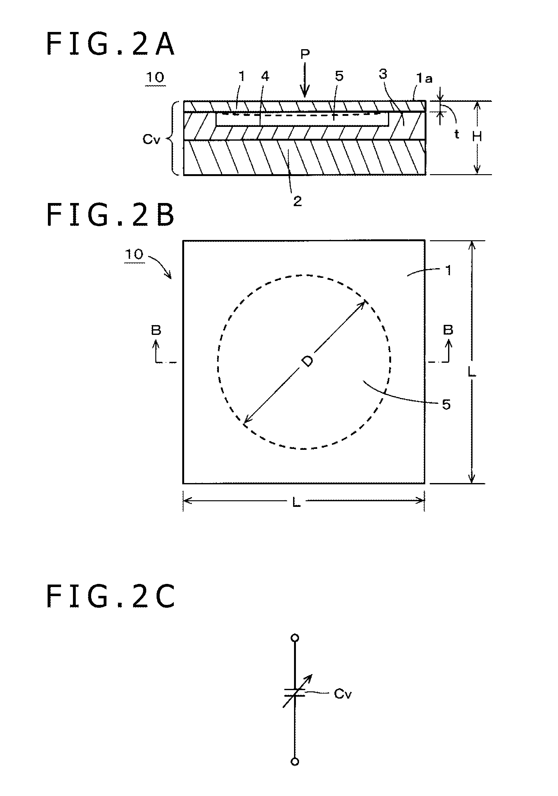
[0071]In the pressure detecting chip 10 of the pressure sensing semiconductor device 100 of the above-described first embodiment, when the thickness “t” of the single-crystal silicon forming the first electrode 1, to which pressure is applied, is changed, the amount of bending of the first electrode 1 depending on the applied pressure also varies. Therefore, by selectively determining the thickness “t” of the first electrode 1, the change characteristic of the capacitance Cv of the pressure detecting chip 10 as a function of the applied pressure P can be varied.

[0072]FIG. 3 is a characteristic diagram showing an example of the change characteristic of the capacitance Cv as a function of the pressure applied to the pressure detecting chip 10. As shown in FIG. 3, when the thickness “t” of the first electrode 1 is t1, the change characteristic of the capacitance Cv of the pressure detecting chip 10 as a function of the applied pressure is as shown by a curve 40.

[0073]When the thickness...


PUM


Abstract

A capacitive pressure sensing semiconductor device is provided, which has pressure resistance against pressure applied by a pressing member and can detect the pressure surely and efficiently. The pressure sensing semiconductor device includes a pressure detecting part, which detects pressure as a change in capacitance, and a package that receives the pressure detecting part within. The pressure detecting part includes a first electrode and a second electrode disposed to oppose the first electrode, with a determined distance therebetween. Capacitance is formed between the first electrode and the second electrode, and changes according to a change in said distance caused by pressure transmitted to the first electrode by a pressing member. The package also includes a pressure transmitting member that transmits, to the first electrode of the pressure detecting part, the pressure applied by the pressing member.

Description

CROSS-REFERENCE(S) TO RELATED APPLICATION(S)[0001]The present application claims priority under 35 U.S.C. 119(a) of Japanese Application No. 2012-015254, filed Jan. 27, 2012, the entire content of which is incorporated herein by reference.BACKGROUND[0002]1. Technical Field[0003]This invention relates to a capacitive pressure sensing semiconductor device that detects pressure applied from the external as change in capacitance.[0004]2. Description of the Related Art[0005]As one example of a position input device used as an input device for a personal computer and so forth, a device is known that consists of a position indicator having a pen-like shape, for example, and including a writing pressure detector, and a position detecting device having an input surface on which pointing operation and input of characters, figures, etc. are performed with the position indicator.[0006]As the writing pressure detector of the position indicator, a capacitance-variable capacitor, for example, like...

Claims


Application Information

Patent Timeline
Patent Type & Authority Applications(United States)
IPC IPC(8): H01L29/84
CPCH01L29/84G01L9/12G01L1/148G01L9/0073G06F3/03545G01L19/06
Inventor HORIE, TOSHIHIKOTAKIGUCHI, HIDETAKA
Owner WACOM CO LTD
Features
  • Generate Ideas
  • Intellectual Property
  • Life Sciences
  • Materials
  • Tech Scout
  • Unparalleled Data Quality
  • Higher Quality Content
  • 60% Fewer Hallucinations
Learn More