Reference voltage generation circuit

Inactive Publication Date: 2014-08-28
ABLIC INC
View PDF4 Cites 4 Cited by
  • Summary
  • Abstract
  • Description
  • Claims
  • Application Information

AI Technical Summary

Benefits of technology

The present invention is about a way to select the best reference voltage from multiple circuits that may have fluctuations in manufacturing steps and reference voltage. The result is that the reference voltage generation circuit can have flat temperature characteristics. This helps to ensure consistent and reliable operation.

Problems solved by technology

Sho 59-200320 has a problem in that the threshold voltages of the transistors may fluctuate due to fluctuations in manufacturing step in a semiconductor manufacturing process and the reference voltage VREF may change due to temperature.

Method used


Image

  • Reference voltage generation circuit
  • Reference voltage generation circuit
  • Reference voltage generation circuit

Examples


Embodiment Construction

[0017]Exemplary embodiments of the present invention are described below with reference to the accompanying drawings.

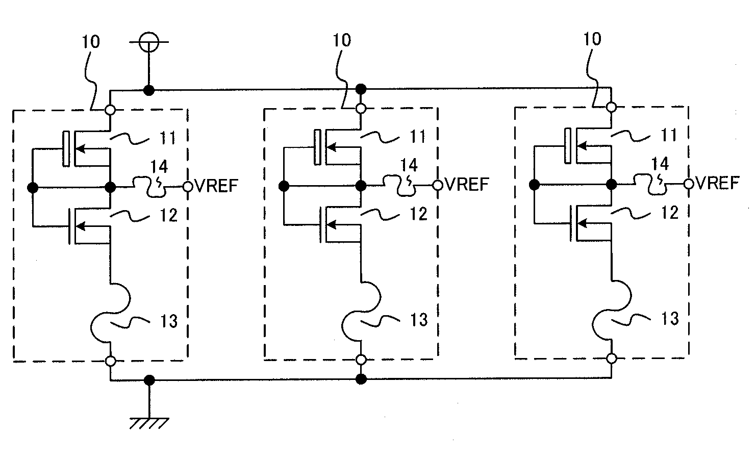
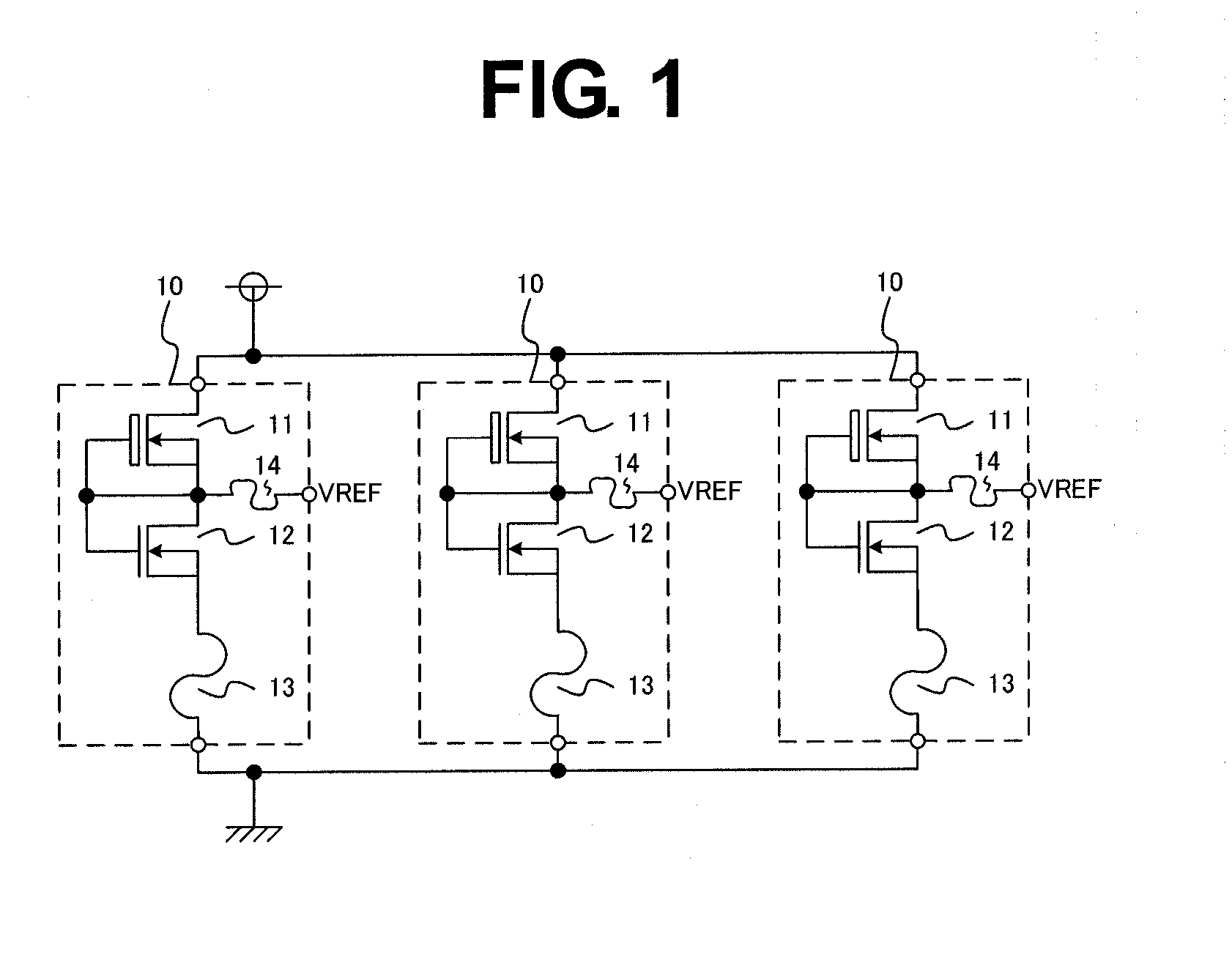
[0018]First, a configuration of a reference voltage generation circuit is described below with reference to FIG. 1.

[0019]The reference voltage generation circuit includes three unit reference voltage generation circuits 10.

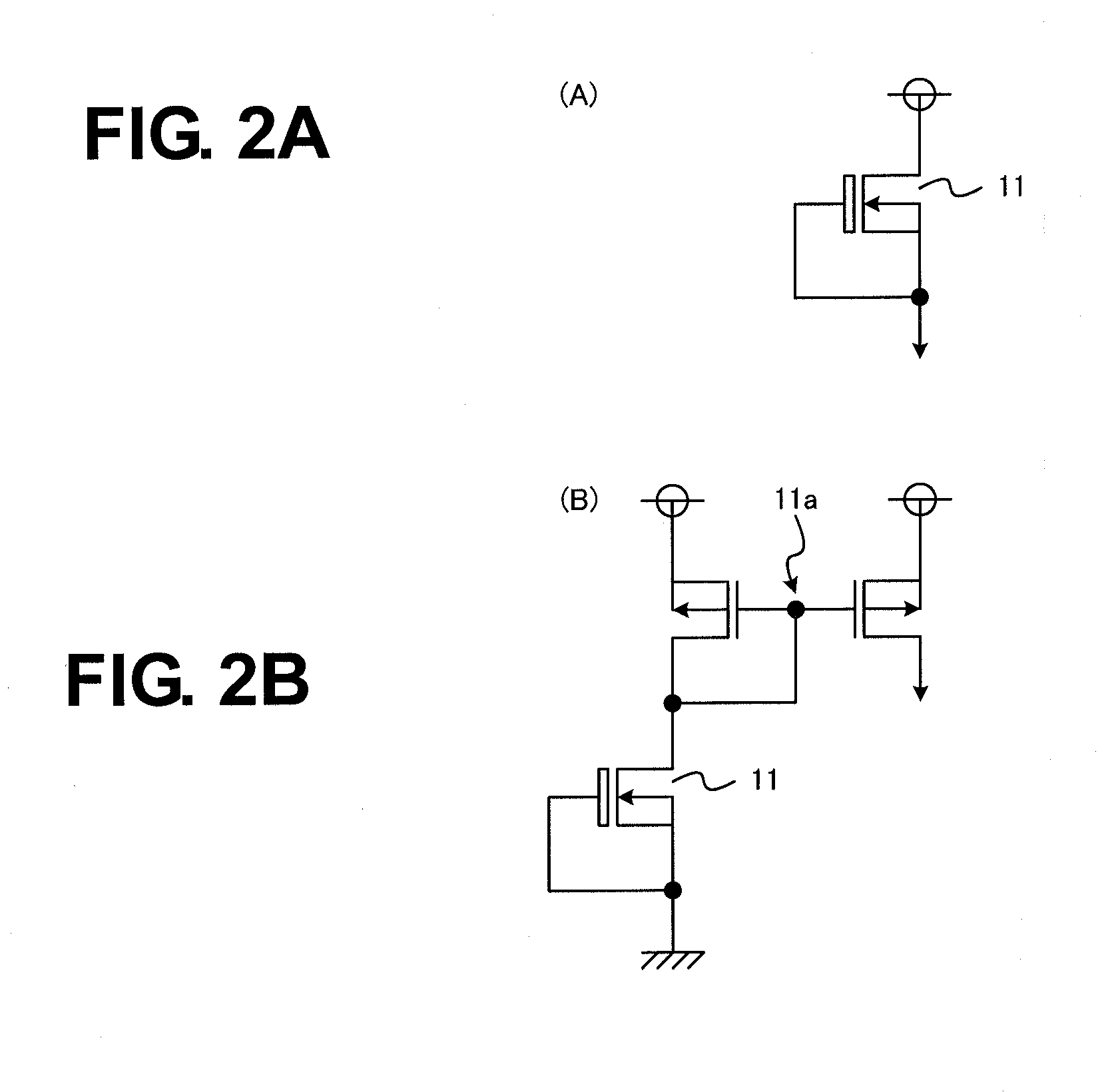
[0020]Each of the unit reference voltage generation circuits 10 includes a depletion type NMOS transistor (D-type NMOS transistor) 11, an enhancement type NMOS transistor (E-type NMOS transistor) 12, and fuses 13 and 14.

[0021]In the reference voltage generation circuit, power supply terminals of the three unit reference voltage generation circuits 10 are each connected to a power supply terminal of a semiconductor device. Ground terminals of the three unit reference voltage generation circuits 10 are each connected to a ground terminal of the semiconductor device. In other words, the three unit reference voltage generation circuits 10 are connected ...


PUM


Abstract

Provided is a reference voltage generation circuit that has a flat temperature characteristic even when there are fluctuations in manufacturing step. After a semiconductor manufacturing process is finished, electrical characteristics of a semiconductor device are evaluated. Temperature characteristic of each reference voltage (VREF) of three unit reference voltage generation circuits (10) is evaluated. Then only a unit reference voltage generation circuit (10) having the most flat temperature characteristics is selected from among the three unit reference voltage generation circuits (10). Only fuses (13, 14) of the selected unit reference voltage generation circuit (10) are not cut, but other fuses (13, 14) are cut. Accordingly only the selected unit reference voltage generation circuit (10) operates, and the other unit reference voltage generation circuits (10) do not operate.

Description

BACKGROUND OF THE INVENTION[0001]1. Field of the Invention[0002]The present invention relates to a reference voltage generation circuit mounted on a semiconductor device, for generating a reference voltage.[0003]2. Description of the Related Art[0004]In recent years, advanced electronic devices have been marketed all over the world and used in various environments. For example, electronic devices are used also in frigid and heavy snowfall areas, tropical areas right on the equator, and other areas. The electronic devices are required to operate normally in almost any temperature environment of human life. Characteristics of a semiconductor device mounted on an electronic device are thus required not to change due to temperature. One reason for deterioration of temperature characteristics of such semiconductor device is that a reference voltage generated by a reference voltage generation circuit in the semiconductor device changes due to temperature.[0005]A related-art reference volt...

Claims


Application Information

Patent Timeline
IPC IPC(8): H03K3/011
CPCH03K3/011G05F3/24
Inventor YOSHINO, HIDEO
Owner ABLIC INC
Why Eureka
Try Eureka