Methods and systems for electric field deposition of nanowires and other devices

a technology of nanowires and electric field, applied in the field of nanostructures, can solve the problems of not scaling well to large area substrates, current deposition techniques that limit the scalability of large-area substrates, and current deposition techniques such as integrated circuits, dies, optical components, etc., to achieve enhanced and guided nanowire positioning, enhance and guide nanowire positioning

Active Publication Date: 2014-11-13
SHARP KK
View PDF4 Cites 3 Cited by
  • Summary
  • Abstract
  • Description
  • Claims
  • Application Information

AI Technical Summary

Benefits of technology

[0017]In another implementation, a deposition system includes a substrate having a surface and an electrode pair. The electrode pair includes a first electrode and a second electrode that are coaxially aligned on the surface. The first electrode has a first end and the second electrode has a second end. The first end and the second end are adjacently positioned and separated by a first distance on the surface of the substrate. The electrode pair is configured to receive an electrical signal to generate an electric field to associate at least one nanowire with the electrode pair. The first end and the second end are each non-square shaped and are configured to enhance and guide nanowire positioning on the electrode pair.
[0018]In another implementation, a technique for deposition of nanostructures is provided. An electrical signal is received at a first electrode and a second electrode of an electrode pair that are coaxially aligned on a surface of a substrate to generate an electric field with the electrode pair to associate at least one nanowire from a suspension with the electrode pair. The first electrode has a first end and the second electrode has a second end. The first end and the second end are adjacently positioned and separated by a first distance on the surface of the substrate. The first end and the second end are each non-square shaped and are configured to enhance and guide nanowire positioning on the electrode pair. The at least one nanowire is locked to the surface of the substrate.

Problems solved by technology

A major impediment to the emergence of this new generation of electronic devices based on nanostructures is the ability to effectively align and deposit the nanostructures on various surfaces, such as substrates.
Electric fields enable the alignment of nanowires suspended in a liquid, but current deposition techniques pose stringent constraints on their scalability to large area substrates.
Likewise, current techniques for depositing electrical devices, such as integrated circuits, dies, optical components, etc., do not scale well to large area substrates.

Method used


Image

  • Methods and systems for electric field deposition of nanowires and other devices
  • Methods and systems for electric field deposition of nanowires and other devices
  • Methods and systems for electric field deposition of nanowires and other devices

Examples


example embodiments

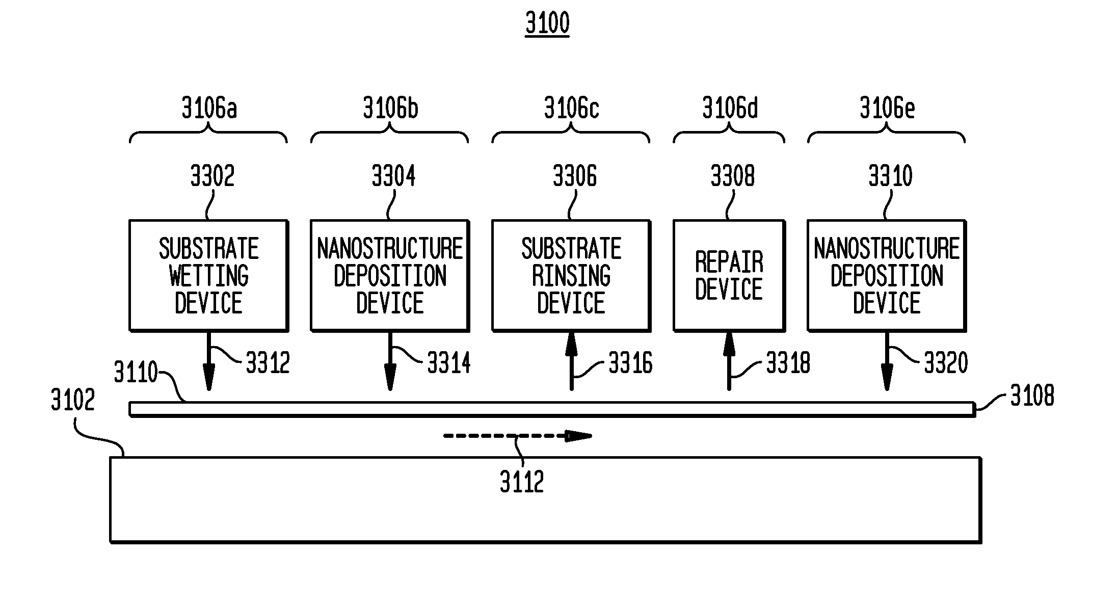
[0346]In an embodiment, a method for deposition of nanostructures to the surface of a substrate comprises: selecting a first solvent having properties that enable dielectrophoretic pinning of nanowires on electrodes of a substrate without the nanowires sticking to the substrate, selecting a second solvent having properties that enable the nanowires to lock to the substrate, flowing a first suspension that includes the first solvent and the nanowires over the substrate to enable the nanowires to be pinned to the substrate, flowing a second suspension that includes the second solvent over the substrate to enable the nanowires to lock to the substrate, and drying the substrate.

[0347]The method may further comprise rinsing the substrate subsequently to said flowing the first suspension.

[0348]The first solvent may be selected to include isopropyl alcohol and water.

[0349]The first solvent may be selected to include isopropyl alcohol.

[0350]At least one of the first and second solvents may ...


PUM

PropertyMeasurementUnit
velocityaaaaaaaaaa
length:widthaaaaaaaaaa

Abstract

Methods, systems, and apparatuses for nanowire deposition are provided. A deposition system includes an enclosed flow channel, an inlet port, and an electrical signal source. The inlet port provides a suspension that includes nanowires into the channel. The electrical signal source is coupled to an electrode pair in the channel to generate an electric field to associate at least one nanowire from the suspension with the electrode pair. The deposition system may include various further features, including being configured to receive multiple solution types, having various electrode geometries, having a rotatable flow channel, having additional electrical conductors, and further aspects.

Description

[0001]This application is a divisional application of U.S. patent application Ser. No. 13 / 322,117, filed on Nov. 22, 2011, which is the U.S. national phase of international application PCT / US2010 / 036065 filed May 25, 2010, which designated the U.S. and claims priority to U.S. Provisional Application No. 61 / 181,229, filed on May 26, 2009, each of which is incorporated by reference herein in its entirety.BACKGROUND OF THE INVENTION[0002]1. Field of the Invention[0003]The present invention relates to nanostructures, and more particularly, to methods and systems for the deposition of nanostructures and electrical devices.[0004]2. Background of the Invention[0005]Nanostructures, such as nanowires, have the potential to facilitate a whole new generation of electronic devices. A major impediment to the emergence of this new generation of electronic devices based on nanostructures is the ability to effectively align and deposit the nanostructures on various surfaces, such as substrates. Ele...

Claims


Application Information

Patent Timeline
Patent Type & Authority Applications(United States)
IPC IPC(8): H01L21/677
CPCH01L21/67703C25D13/02B82Y10/00B82Y40/00C25D13/22C25D17/12H01L21/02603H01L21/326H01L29/0665H01L29/0673Y10S977/89Y10S977/936
Inventor FREER, ERIKHAMILTON, JAMES M.STUMBO, DAVID P.KOMIYA, KENJISHIBATA, AKIHIDE
Owner SHARP KK
Why Eureka
Try Eureka