Methods and systems for electric field deposition of nanowires and other devices

a technology of nanowires and electric field, applied in the field of nanostructures, can solve the problems of not scaling well to large area substrates, current deposition techniques, integrated circuits, optical components, etc., and achieve the effects of enhancing and guiding nanowire positioning

Inactive Publication Date: 2012-05-31
SHARP KK +1
View PDF3 Cites 46 Cited by
  • Summary
  • Abstract
  • Description
  • Claims
  • Application Information

AI Technical Summary

Benefits of technology

[0017]In another implementation, a deposition system includes a substrate having a surface and an electrode pair. The electrode pair includes a first electrode and a second electrode that are coaxially aligned on the surface. The first electrode has a first end and the second electrode has a second end. The first end and the second end are adjacently positioned and separated by a first distance on the surface of the substrate. The electrode pair is configured to receive an electrical signal to generate an electric field to associate at least one nanowire with the electrode pair. The first end and the second end are each non-square shaped and are configured to enhance and guide nanowire positioning on the electrode pair.
[0018]In another implementation, a technique for deposition of nanostructures is provided. An electrical signal is received at a first electrode and a second electrode of an electrode pair that are coaxially aligned on a surface of a substrate to generate an electric field with the electrode pair to associate at least one nanowire from a suspension with the electrode pair. The first electrode has a first end and the second electrode has a second end. The first end and the second end are adjacently positioned and separated by a first distance on the surface of the substrate. The first end and the second end are each non-square shaped and are configured to enhance and guide nanowire positioning on the electrode pair. The at least one nanowire is locked to the surface of the substrate.

Problems solved by technology

A major impediment to the emergence of this new generation of electronic devices based on nanostructures is the ability to effectively align and deposit the nanostructures on various surfaces, such as substrates.
Electric fields enable the alignment of nanowires suspended in a liquid, but current deposition techniques pose stringent constraints on their scalability to large area substrates.
Likewise, current techniques for depositing electrical devices, such as integrated circuits, dies, optical components, etc., do not scale well to large area substrates.

Method used


Image

  • Methods and systems for electric field deposition of nanowires and other devices
  • Methods and systems for electric field deposition of nanowires and other devices
  • Methods and systems for electric field deposition of nanowires and other devices

Examples


Embodiment Construction

I. Introduction

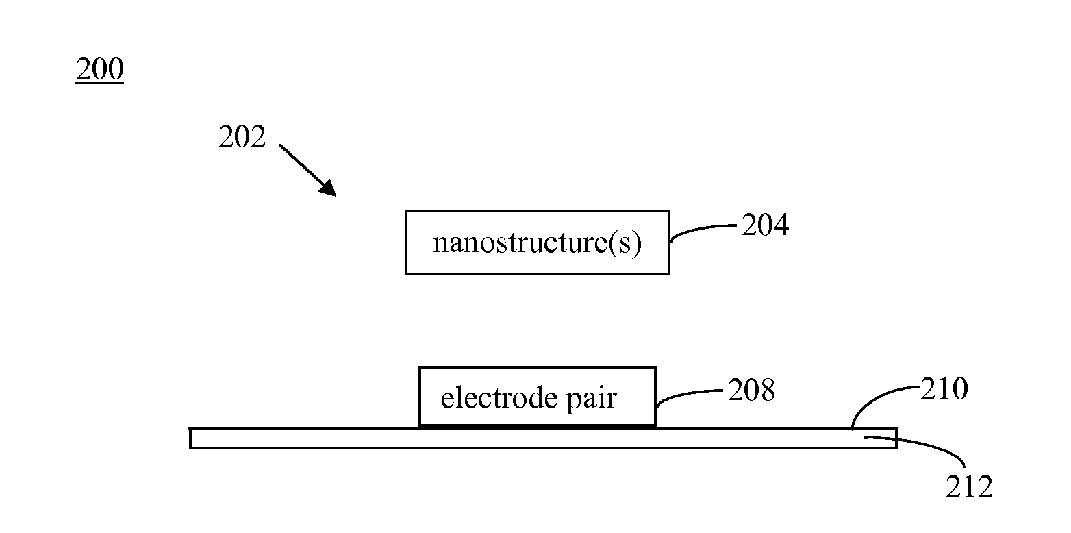
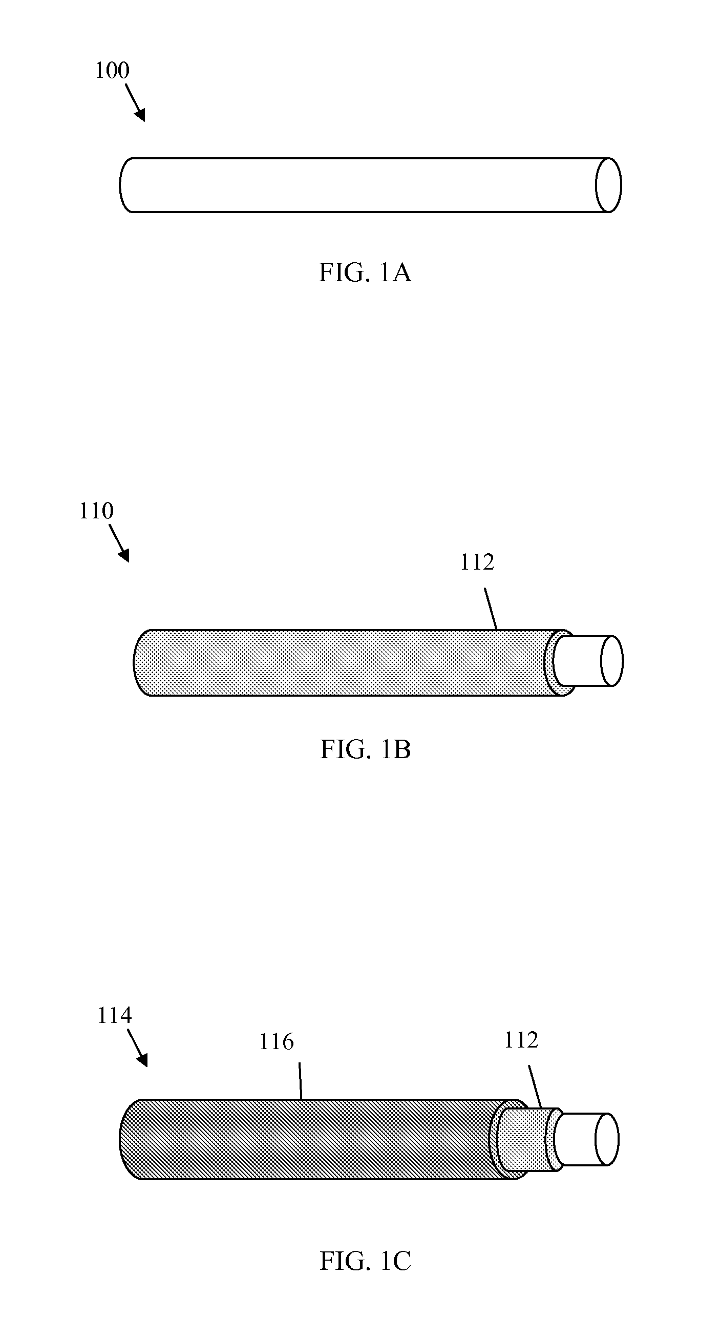
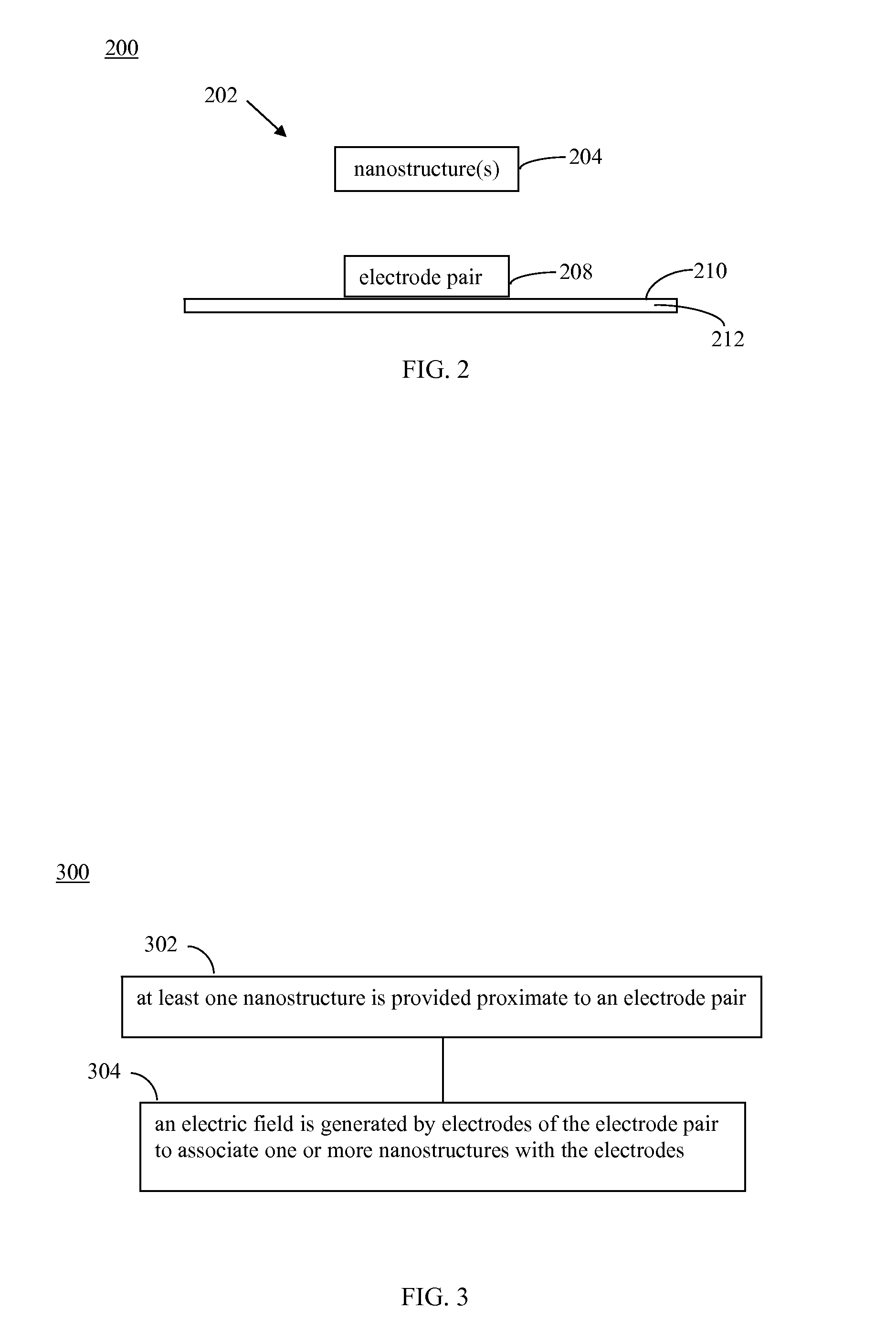
[0097]It should be appreciated that the particular implementations shown and described herein are examples of the invention and are not intended to otherwise limit the scope of the present invention in any way. Indeed, for the sake of brevity, conventional electronics, manufacturing, semiconductor devices, and nanowire (NW), nanorod, nanotube, and nanoribbon technologies and other functional aspects of the systems (and components of the individual operating components of the systems) may not be described in detail herein. Furthermore, for purposes of brevity, the invention is frequently described herein as pertaining to nanowires.

[0098]It should be appreciated that although nanowires are frequently referred to, the techniques described herein are also applicable to other nanostructures, such as nanorods, nanotubes, nanotetrapods, nanoribbons and / or combinations thereof. It should further be appreciated that the manufacturing techniques described herein could be used t...


PUM

PropertyMeasurementUnit
length:widthaaaaaaaaaa
aspect ratioaaaaaaaaaa

Abstract

Methods, systems, and apparatuses for nanowire deposition are provided. A deposition system includes an enclosed flow channel, an inlet port, and an electrical signal source. The inlet port provides a suspension that includes nanowires into the channel. The electrical signal source is coupled to an electrode pair in the channel to generate an electric field to associate at least one nanowire from the suspension with the electrode pair. The deposition system may include various further features, including being configured to receive multiple solution types, having various electrode geometries, having a rotatable flow channel, having additional electrical conductors, and further aspects.

Description

[0001]This application is the U.S. national phase of international application PCT / US2010 / 036065 filed May 25, 2010, which designated the U.S. and claims priority to U.S. Provisional Application No. 61 / 181,229, filed on May 26, 2009, each of which is incorporated by reference herein in its entirety.BACKGROUND OF THE INVENTION[0002]1. Field of the Invention[0003]The present invention relates to nanostructures, and more particularly, to methods and systems for the deposition of nanostructures and electrical devices.[0004]2. Background of the Invention[0005]Nanostructures, such as nanowires, have the potential to facilitate a whole new generation of electronic devices. A major impediment to the emergence of this new generation of electronic devices based on nanostructures is the ability to effectively align and deposit the nanostructures on various surfaces, such as substrates. Electric fields enable the alignment of nanowires suspended in a liquid, but current deposition techniques po...

Claims


Application Information

Patent Timeline
Patent Type & Authority Applications(United States)
IPC IPC(8): B05D5/00B05C9/12B05D3/14B82Y30/00
CPCB82Y10/00B82Y40/00C25D13/02H01L21/67703C25D17/12H01L29/0665H01L29/0673C25D13/22H01L21/02603H01L21/326Y10S977/89Y10S977/936
Inventor FREER, ERIKHAMILTON, JAMES M.STUMBO, DAVID P.KOMIYA, KENJISHIBATA, AKIHIDE
Owner SHARP KK
Why Eureka
Try Eureka