Transparent conducting film and preparation method thereof

a technology of transparent conducting film and conducting film, which is applied in the direction of non-metal conductors, sustainable manufacturing/processing, and final product manufacturing, etc., can solve the problems of reducing sn, affecting the performance of the product, and affecting the quality of the product, so as to achieve excellent elasticity and adhesive strength, excellent conductivity and transmittance, and low haze value

Active Publication Date: 2015-07-09
LG CHEM LTD
View PDF3 Cites 10 Cited by
  • Summary
  • Abstract
  • Description
  • Claims
  • Application Information

AI Technical Summary

Benefits of technology

[0015]A transparent conductive film according to an exemplary embodiment of the present application comprises a compound having a crystalline structure and represented by Chemical Formula 1 and thus has excellent conductivity and transmittance. Further, the transparent conductive film according to an exemplary embodiment of the present application has excellent elasticity and adhesive strength. Furthermore, the transparent conductive film according to an exemplary embodiment of the present application has a low haze value. Therefore, the transparent conductive film according to the present application can be applied as a technology substituting for conventional ITO conductive films.

Problems solved by technology

However, the ITO has the disadvantage of high price since In is one of rare elements, and if it is exposed to hydrogen plasma often used in a flat panel display manufacturing process, In or Sn is reduced and electrical and optical properties may be deteriorated.

Method used


Image

  • Transparent conducting film and  preparation method thereof
  • Transparent conducting film and  preparation method thereof
  • Transparent conducting film and  preparation method thereof

Examples


example

Example 1

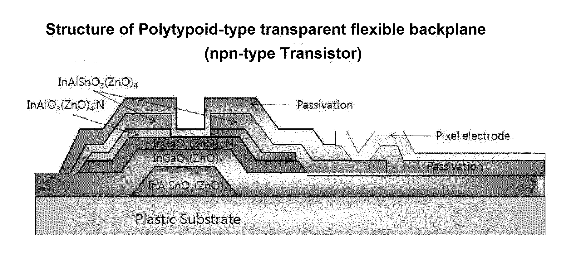
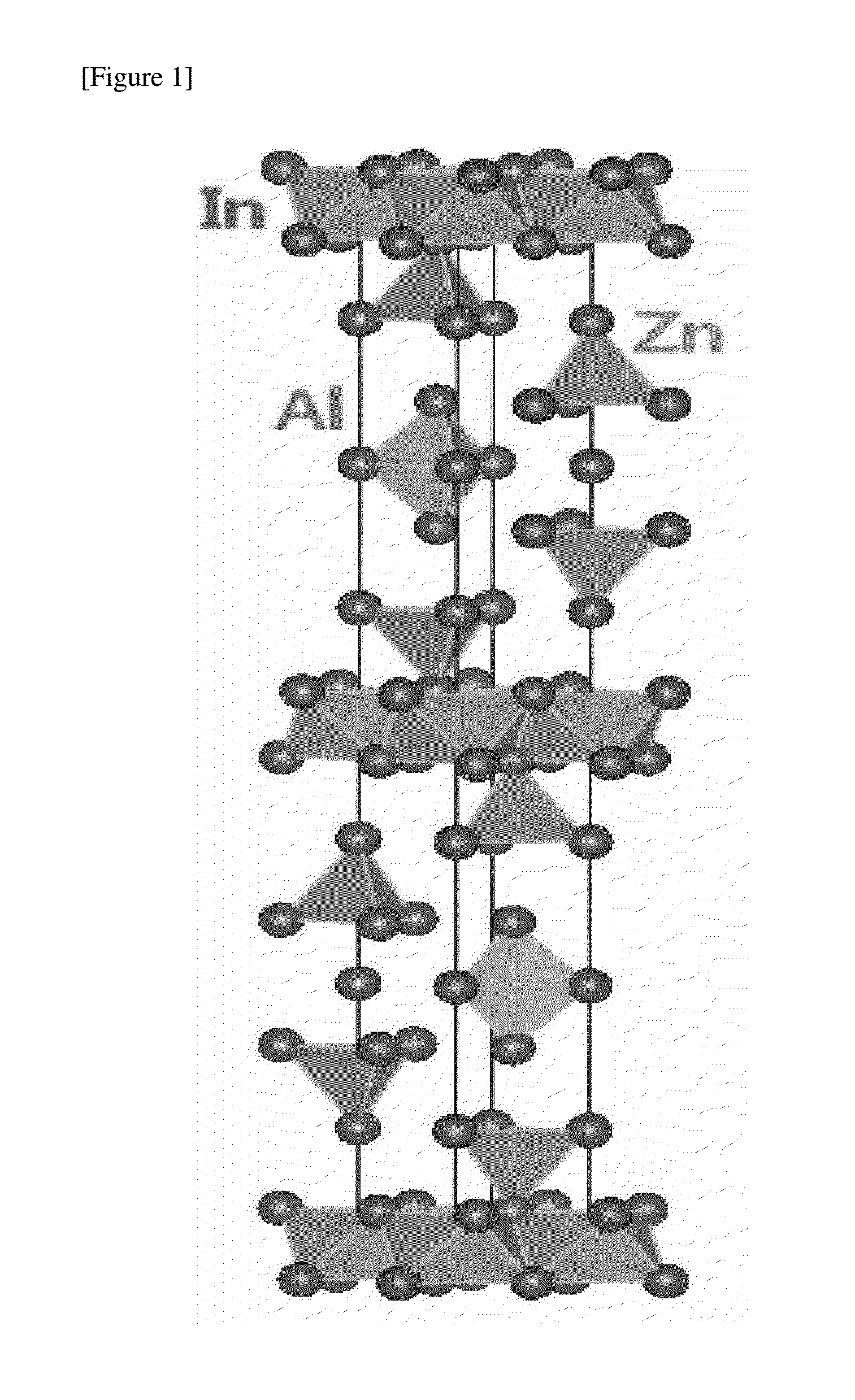
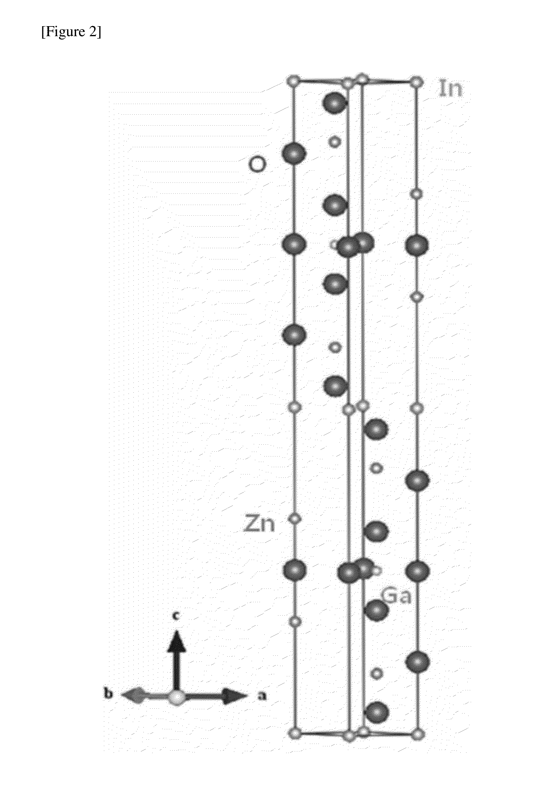
[0096]A conductive film containing InAlO3(ZnO)4 or InGaO3(ZnO)4 was prepared to a thickness of 50 nm. A roll-to-roll process was applied using a DC / RF magnetron sputtering evaporator. A vacuum level of a chamber system was usually maintained at 10−5 torr. In2O3, Al2O3, ZnO, Ga2O3 sputter targets (1,600×125 mm2, ˜3.5 KW power applied) were installed at the evaporator and spaced 70 to 75 mm apart from a plastic substrate (eg. PET, PC having a width of 1,050 mm). By additionally introducing an O2 gas, an oxygen atoms insufficient for vapor deposition were supplied. As a result, a transparent conductive film containing InAlO3(ZnO)4 and InGaO3(ZnO)4 at a qualitative ratio was obtained.

[0097]Optical transmittance of the conductive film was obtained by a hybrid method (HSE06 method) and a result thereof is illustrated in FIG. 7. Electrical conductivity is illustrated in FIG. 8.

[0098]As confirmed in the above results, transmittance of visible light was as high as 87 to 91%. Further...


PUM

PropertyMeasurementUnit
electronic energy band gapaaaaaaaaaa
light transmittanceaaaaaaaaaa
hole mobilityaaaaaaaaaa

Abstract

There are provided a transparent conductive film and a method for preparing the same. The transparent conductive film of the present application comprises a compound having a crystalline structure and represented by Chemical Formula 1 and thus can be applied as a technology substituting for conventional ITO conductive films.

Description

TECHNICAL FIELD[0001]This application claims priority to and the benefit of Korean Patent Application No. 10-2012-0103498 filed in the Korean Intellectual Property Office on Sep. 18, 2012, the entire contents of which are incorporated herein by reference.[0002]The present invention relates to a transparent conductive film and a method for preparing the same.BACKGROUND ART[0003]A transparent conductive film refers to a thin film having high light transmittance and an electrically conductive property and has been widely used as a voltage apply type common electrode or pixel electrode of a liquid crystal display, an electrochromic display (ECD, an organic electroluminescence device, a solar cell, a plasma display panel, a flexible display, electronic paper, a touch panel, and the like.[0004]As for transparent conducting oxides (TCOs), it is important to design a material which transmits light in the visible ray area and has high conductivity. In order to be transparent in the visible r...

Claims


Application Information

Patent Timeline
Patent Type & Authority Applications(United States)
IPC IPC(8): H01L29/786C01G15/00H01L29/51H01L29/45H01L29/49
CPCH01L29/7869H01L29/45H01L29/4908C01P2006/40H01L29/517H01L29/78696C01G15/006H01L29/4966H01B1/08H01L31/022466C01P2002/76C01P2002/77Y02E10/549Y02P70/50H10K30/82H10K50/81H01B5/14H01B13/00
Inventor SHIN, DONGMYUNGKIMCHUNG, CHANYEUP
Owner LG CHEM LTD
Why Eureka
Try Eureka