Current mirror circuit and receiver using the same

a current mirror and receiver technology, applied in the direction of process and machine control, transmission monitoring, instruments, etc., can solve the problem of limited input current range, achieve high accuracy amplify a current, prevent an increase in the chip area, and wide input current range

Active Publication Date: 2015-10-01
MEGACHIPS
View PDF2 Cites 5 Cited by
  • Summary
  • Abstract
  • Description
  • Claims
  • Application Information

AI Technical Summary

Benefits of technology

[0009]One or more embodiments of the present invention generally relate to a current mirror circuit that can highly accurately amplify a current while preventing an increase in the chip area and handling a wide range of input current.

Problems solved by technology

Necessarily, the range of the input current is limited.

Method used


Image

  • Current mirror circuit and receiver using the same
  • Current mirror circuit and receiver using the same
  • Current mirror circuit and receiver using the same

Examples


Embodiment Construction

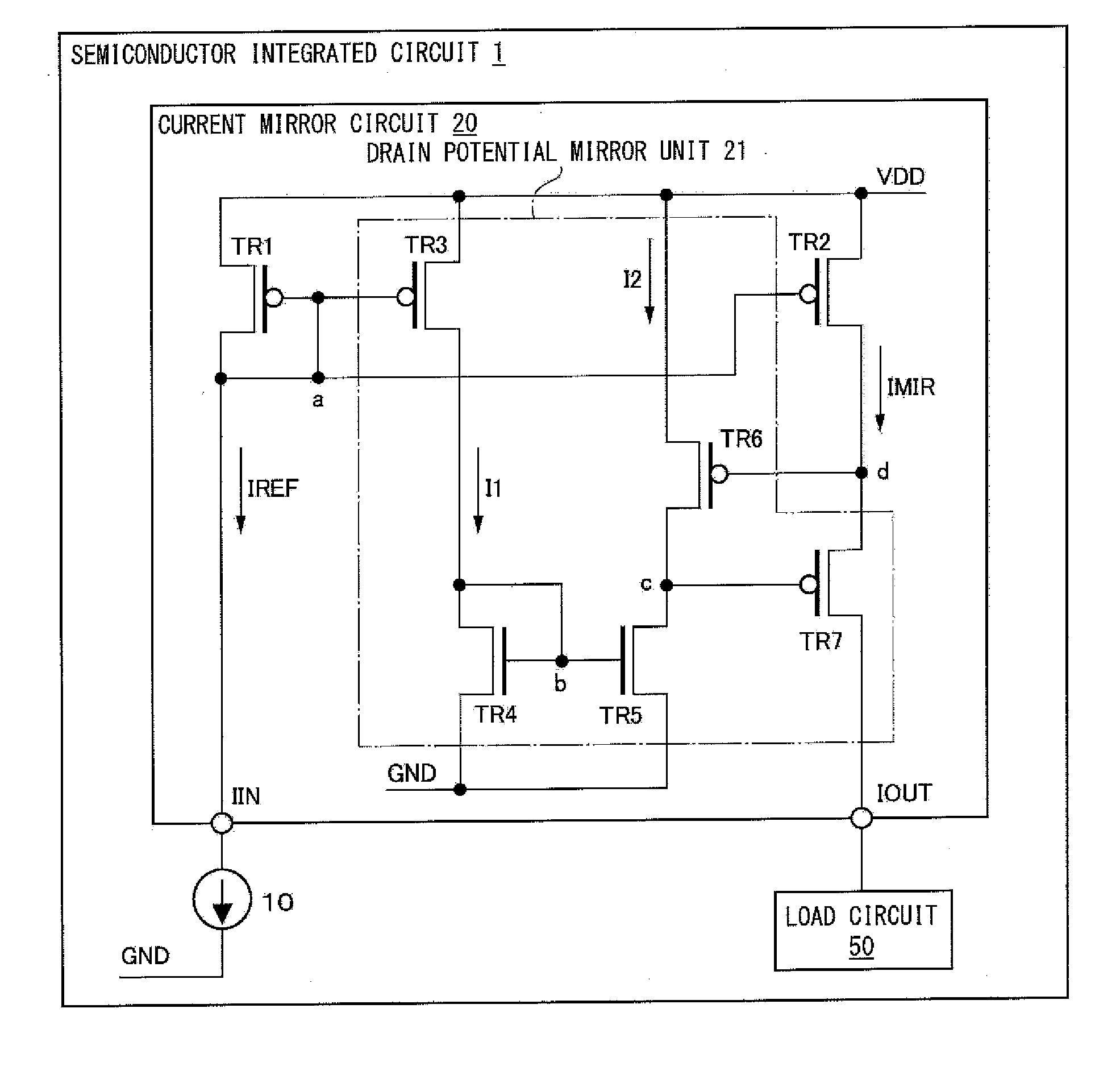
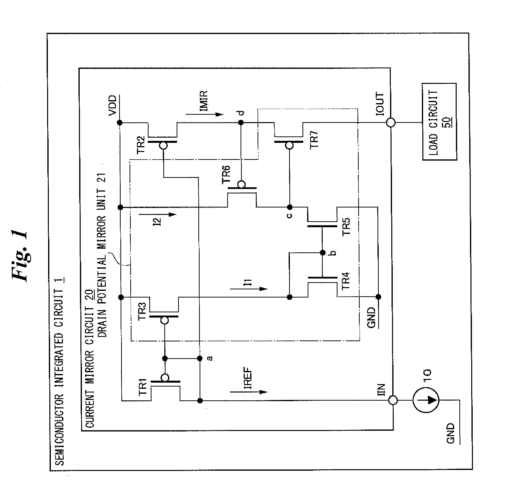
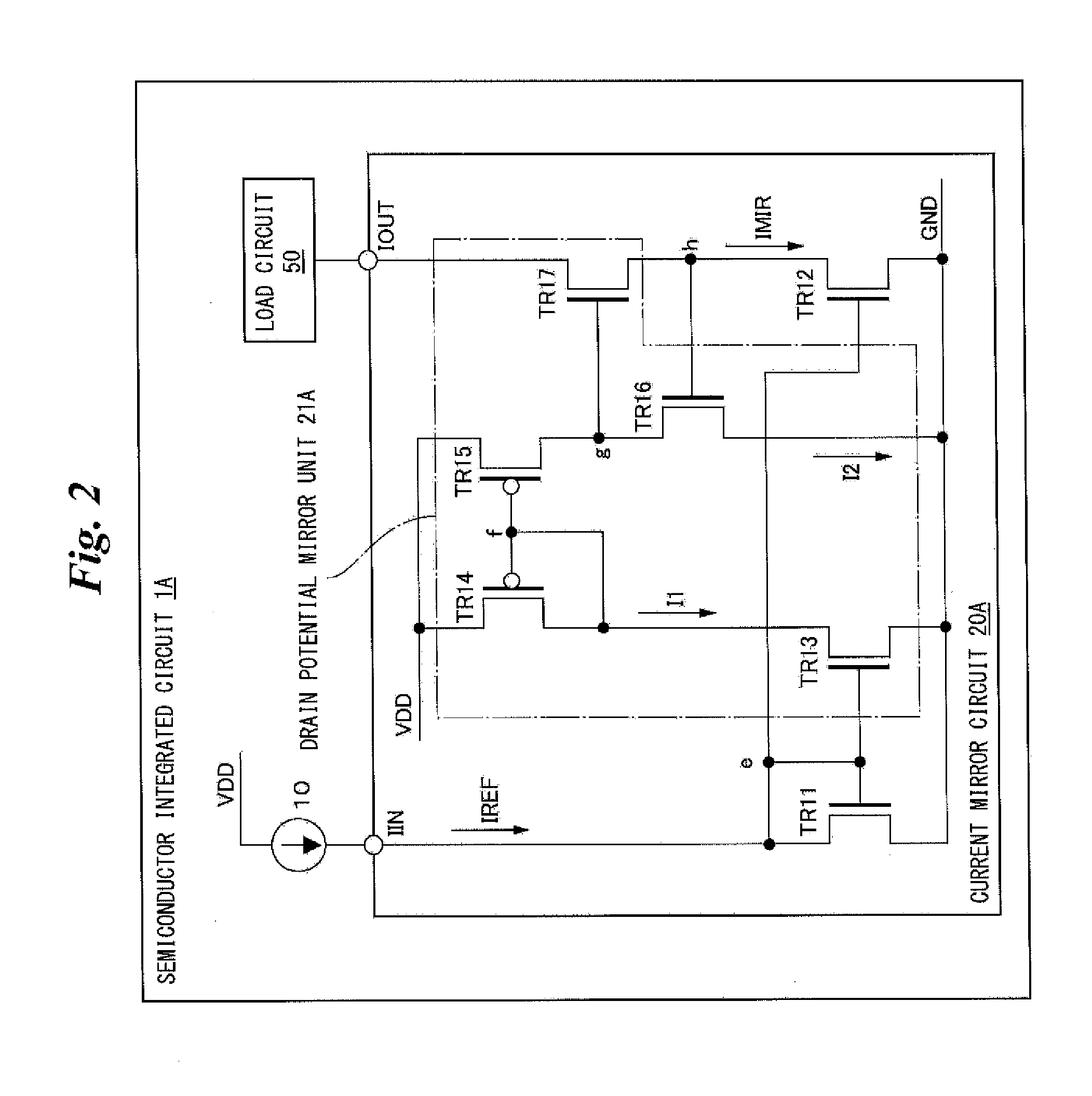
[0046]Hereinafter, embodiments of the present invention will be described with reference to the drawings. In embodiments of the invention, numerous specific details are set forth in order to provide a more thorough understanding of the invention. However, it will be apparent to one of ordinary skill in the art that the invention may be practiced without these specific details. In other instances, well-known features have not been described in detail to avoid obscuring the invention. FIG. 1 is a diagram showing an example of a semiconductor integrated circuit (IC) according to one or more embodiments of the present invention. As shown in FIG. 1, a semiconductor IC 1 may comprise a current source 10, a current mirror circuit 20, and a load circuit 50.

[0047]The current source 10 may be, for example, a MOS transistor that generates a reference current IREF in the current mirror circuit 20. The current source 10 may be connected to the drain of a transistor TR1 and the gates of transisto...


PUM


Abstract

A current mirror circuit that amplifies a reference current generated by a current source at a first magnification to supply a mirror current to a load circuit. The current mirror circuit includes a first transistor and a second transistor that share a power supply, and a drain potential mirror unit that amplifies the reference current at a second magnification to generate a first current, that amplifies a generated first current at a third magnification to generate a second current, and that supplies a predetermined potential determined based on the second current to a drain of the second transistor. The mirror current is supplied from the second transistor to the load circuit based on a potential of a gate of the first transistor determined based on the reference current

Description

FIELD OF THE INVENTION[0001]One or more embodiments of the present invention relates to a current mirror circuit and a receiver using a current mirror.BACKGROUND OF THE INVENTION[0002]In the information society, it has become increasingly important to communicate using an optical signal to quickly transmit and receive a larger amount of information. A communication system using such an optical signal may comprise a transmitter, a receiver, and an optical fiber connecting the transmitter and the receiver. In the communication system using the optical signal, the transmitter converts an electrical signal to an optical signal in one of two states “1” and “0” corresponding to the light strength, and the receiver converts the optical signal back to an electrical signal in order to transmit information. Measurement of the strength of the optical signal is important for the receiver in order to accurately read the information indicated by the optical signal.[0003]The receiver in the commun...

Claims


Application Information

Patent Timeline
Patent Type & Authority Applications(United States)
IPC IPC(8): G05F3/26H04B10/60H04B10/079
CPCG05F3/262H04B10/60H04B10/0795H03F3/50H03F2200/474H03F2203/21115H03G3/3084
Inventor YAMAHANA, RYOTA
Owner MEGACHIPS
Why Eureka
Try Eureka