Universal test socket, semiconductor test device, and method of testing semiconductor devices

Active Publication Date: 2019-01-10
SAMSUNG ELECTRONICS CO LTD
View PDF8 Cites 0 Cited by
  • Summary
  • Abstract
  • Description
  • Claims
  • Application Information

AI Technical Summary

Benefits of technology

The patent text describes the development of universal test sockets and test devices that can perform testing on various types of semiconductor devices. These concepts offer an improved and cost-effective way to test semiconductor devices.

Problems solved by technology

Still further, time for attaching and detaching the test socket to a test device takes time.

Method used


Image

  • Universal test socket, semiconductor test device, and method of testing semiconductor devices
  • Universal test socket, semiconductor test device, and method of testing semiconductor devices
  • Universal test socket, semiconductor test device, and method of testing semiconductor devices

Examples


Embodiment Construction

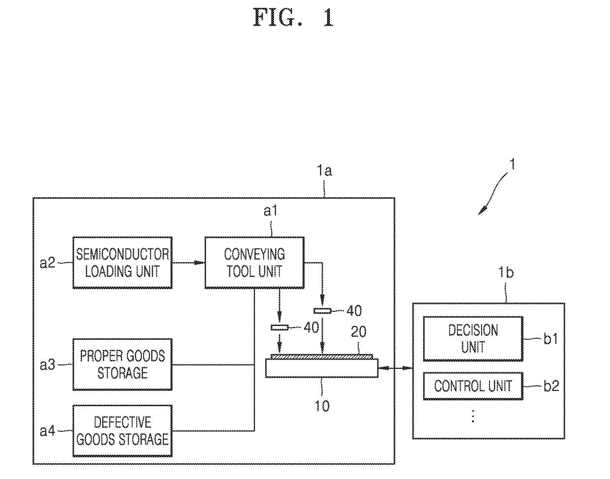
[0024]FIG. 1 is a block diagram of a test device 1 according to an example embodiment of the inventive concepts.

[0025]Referring to FIG. 1, the test device 1 may include a test main body 1a and a test controller 1b for controlling a test performed by the test main body 1a.

[0026]The test main body 1a is a portion where loading and conveying of a semiconductor device 40 to be tested and sorting of proper goods and defective goods are actually performed, and is referred to as a ‘test handler unit’ or a “test handler”. Also, the test controller 1b transmits electric signals to the test main body 1a to determine whether the semiconductor device 40 is proper goods. The test controller 1b may be a processor configured to process computer readable instructions of, for example, a computer program by performing a basic arithmetic and logic operation, and an input / output (I / O) operation of the test device 1, thereby transforming the test controller 1b into a special purpose processor. The comp...


PUM


Abstract

A universal test socket including a first sub-layer including a plurality of first through conductors, the plurality of first through conductors arranged at a first pitch in a first substrate, and a second sub-layer including a plurality of second through conductors, the second sub-layer stacked on the first sub-layer so that the plurality of first through conductors are in contact with the plurality of second through conductors, the plurality of second through conductors arranged at a second pitch in a second substrate, the second pitch being less than or equal to the first pitch may be provided.

Description

CROSS-REFERENCE TO RELATED APPLICATIONS[0001]This application claims priority under 35 U.S.C. § 119 to Korean Patent Application No. 10-2017-0087283, filed on Jul. 10, 2017, in the Korean Intellectual Property Office, the disclosure of which is incorporated herein in its entirety by reference.BACKGROUND[0002]The inventive concepts relate to universal test sockets, semiconductor test devices, and / or methods of testing semiconductor devices, and more particularly, to universal test sockets, semiconductor test devices, and methods of testing semiconductor devices which are applicable to various types of semiconductor devices and are capable of performing test in an improved and / or inexpensive manner.[0003]A semiconductor device has to undergo various tests in order to check its reliability. A test socket used for the test of the semiconductor device includes terminals having one-to-one correspondence with terminals of the semiconductor device. If a semiconductor device to be tested is ...

Claims


Application Information

Patent Timeline
IPC IPC(8): G01R1/073H05K1/11G01R31/26
CPCG01R1/0735H05K1/11H05K2201/10325G01R1/07364G01R31/2601G01R1/0416G01R1/0466G01R1/0483G01R35/00G01R31/2863G01R31/2865G01R1/0433G01R1/06761G01R1/06733G01R31/2886G01R31/01
Inventor YAMADA, DAISUKESHIN, DONG-UHN
Owner SAMSUNG ELECTRONICS CO LTD
Why Eureka
Try Eureka