Semiconductor device

Active Publication Date: 2019-12-19
SK HYNIX INC
View PDF8 Cites 46 Cited by
  • Summary
  • Abstract
  • Description
  • Claims
  • Application Information

AI Technical Summary

Benefits of technology

The present disclosure describes a semiconductor device that includes a cell array with two segments that are refreshed differently. The device has a repair controller that can control the repair of each segment separately based on a fuse address, a row address, a second control signal, and a selection address. The technical effect of this design is that it allows for more efficient repair of the upper and lower segments of the cell array.

Problems solved by technology

However, if a defective or failed cell occurs in at least one memory cell from among a plurality of memory cells, it is impossible for a semiconductor memory device to normally operate, so that the semiconductor memory device having the defective cell is regarded as a defective product and abandoned.
Moreover, as the semiconductor memory device has been developed to have a higher degree of integration at a higher speed, there is a higher possibility of causing defective cells.
Provided that the entirety of the semiconductor memory device is discarded due to a defect generated in only a few memory cells among all memory cells contained in the semiconductor memory device, the discarding of the entirety of the semiconductor memory device is cost ineffective and is far from high product efficiency.

Method used


Image

  • Semiconductor device
  • Semiconductor device
  • Semiconductor device

Examples


Embodiment Construction

[0019]Reference will now be made to embodiments of the present disclosure, examples of which are illustrated in the accompanying drawings. Wherever possible, the same reference numbers are used throughout the drawings to refer to the same or like portions.

[0020]Various embodiments of the present disclosure may be directed to providing a semiconductor device that substantially obviates one or more problems due to limitations and disadvantages of the related art.

[0021]The embodiments of the present disclosure may relate to a semiconductor device for extending a row repair region to another segment region.

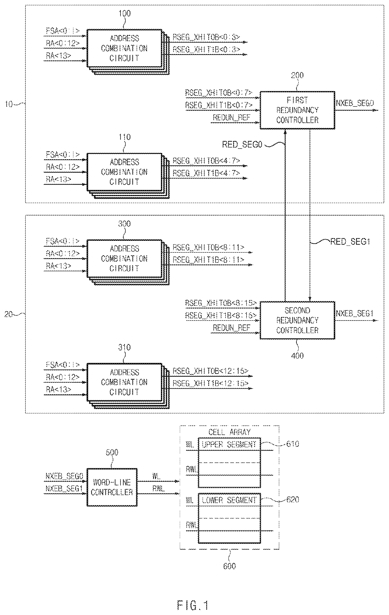
[0022]FIG. 1 is a schematic diagram illustrating a representation of an example of a semiconductor device according to an embodiment of the present disclosure.

[0023]Referring to FIG. 1, the semiconductor device according to an embodiment of the present disclosure may include repair controllers 10 and 20, a word-line controller 500, and a cell array 600.

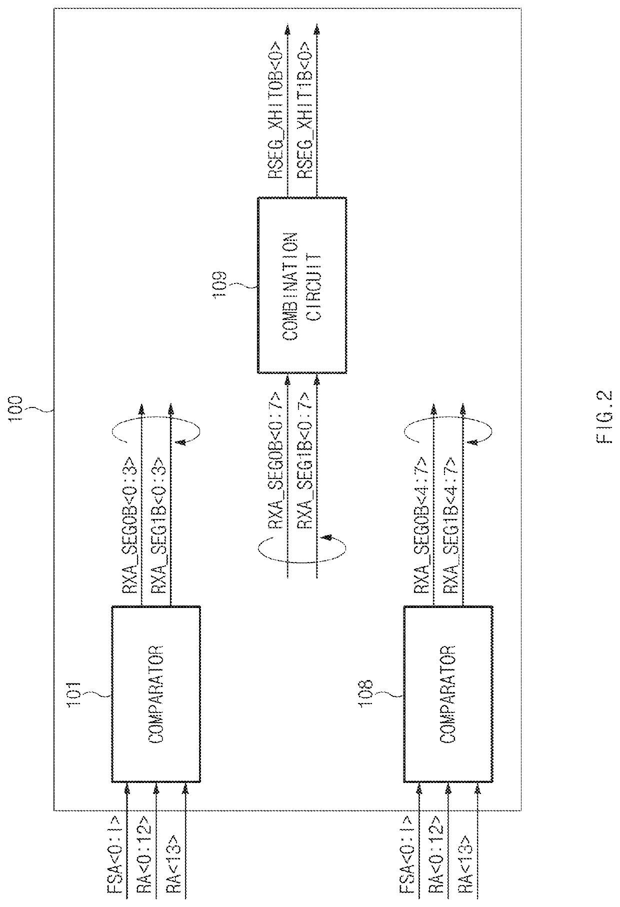
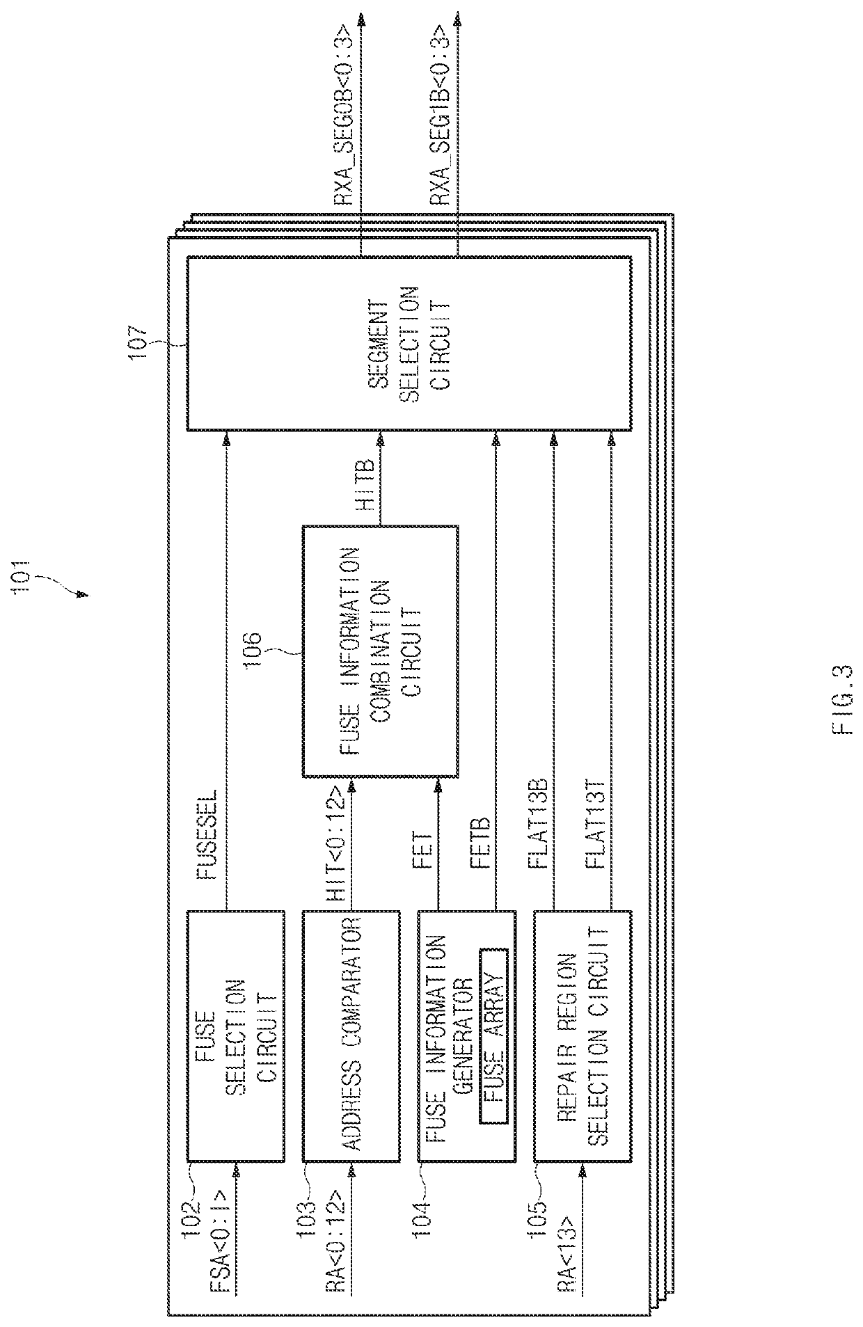
[0024]The repair controller 10 m...


PUM


Abstract

A semiconductor device includes a cell array having an upper segment and a lower segment which are classified according to refresh units. The semiconductor device includes a first repair controller configured to output a first repair signal for controlling a repair operation of the upper segment based on a fuse address, a row address, a second control signal, and selection address being at a first level, and generate a first control signal for controlling a repair operation of the lower segment based on the fuse address, the row address, and selection address.

Description

CROSS-REFERENCE TO RELATED APPLICATION[0001]This application claims priority based upon Korean patent application No. 10-2018-0070045, filed on Jun. 19, 2018, the disclosure of which is hereby incorporated in its entirety by reference herein.BACKGROUND1. Technical Field[0002]Embodiments of the present disclosure generally relate to a semiconductor device, and more particularly, to a technology for a repair circuit configured to replace a defective cell with a redundancy cell and method to replace a defective cell with a redundancy cell.2. Related Art[0003]A semiconductor memory device is constructed of a plurality of memory cells which are arranged in the form of a matrix.[0004]However, if a defective or failed cell occurs in at least one memory cell from among a plurality of memory cells, it is impossible for a semiconductor memory device to normally operate, so that the semiconductor memory device having the defective cell is regarded as a defective product and abandoned.[0005]Mor...

Claims


Application Information

Patent Timeline
IPC IPC(8): G11C11/408G11C11/406
CPCG11C11/406G11C11/4087G11C2211/4065G11C29/70G11C11/40611G11C29/785G11C29/783G11C29/81G11C29/808G11C29/838G11C29/787G11C29/802
Inventor KOO, JA BEOMCHI, SUNG SOO
Owner SK HYNIX INC
Why Eureka
Try Eureka