Supercharge Your Innovation With Domain-Expert AI Agents!

Base material for printed interconnect boards and manufacturing method of printed interconnect boards

a technology manufacturing methods, which is applied in the manufacture of printed circuits, metallic pattern materials, printed circuit details, etc., can solve the problems of reduced size of printed interconnect boards used in devices, inability to generate printed interconnect boards as products, and remarkably dense interconnect density, so as to reduce the variation of plating film thickness, eliminate individual differences in product performance, and enhance productivity

Active Publication Date: 2020-01-09
SUMITOMO ELECTRIC IND LTD +1
View PDF0 Cites 0 Cited by
  • Summary
  • Abstract
  • Description
  • Claims
  • Application Information

AI Technical Summary

Benefits of technology

This patent describes a base material for printed interconnect boards that has a base film and at least one conductive layer layered on top of it. The base material has a regular array of interconnect board pieces with a smaller layered conductive layer area rate in the outer frame region around the product. This design helps to improve the performance and reliability of the printed interconnect boards.

Problems solved by technology

In accordance with that, printed interconnect boards used in devices are reduced in size and the interconnect density becomes remarkably dense and complex.
In some cases, there is a possibility that printed interconnect boards that cannot be used as products are generated.

Method used


Image

  • Base material for printed interconnect boards and manufacturing method of printed interconnect boards
  • Base material for printed interconnect boards and manufacturing method of printed interconnect boards

Examples


first embodiment

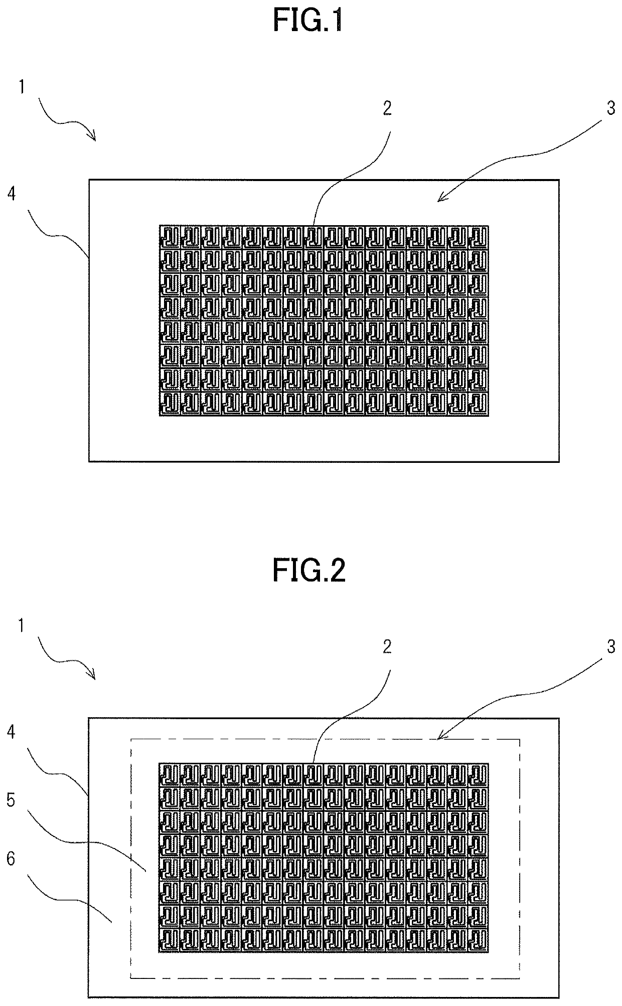
[0029]A base material 1 for printed interconnect boards according to an aspect of the present invention includes a product 3 in which a plurality of interconnect board pieces 2 are arrayed and includes an outer frame region 4 surrounding the product 3, as illustrated in FIG. 1. The outer frame region 4 does not include interconnect board pieces 2, and is separated and removed from the product 3 when the interconnect board pieces 2 are obtained as printed interconnect boards. The interconnect board pieces 2 and the base material 1 for printed interconnect boards are both formed to be substantially rectangular in a plan view, and several tens to several hundreds of interconnect board pieces 2 are disposed on the base material 1 for printed interconnect boards.

[0030](Product)

[0031]The product 3 is composed of the plurality of interconnect board pieces 2 that are regularly arrayed. Small printed interconnect boards manufactured in such a configuration are often small coils or the like, ...

second embodiment

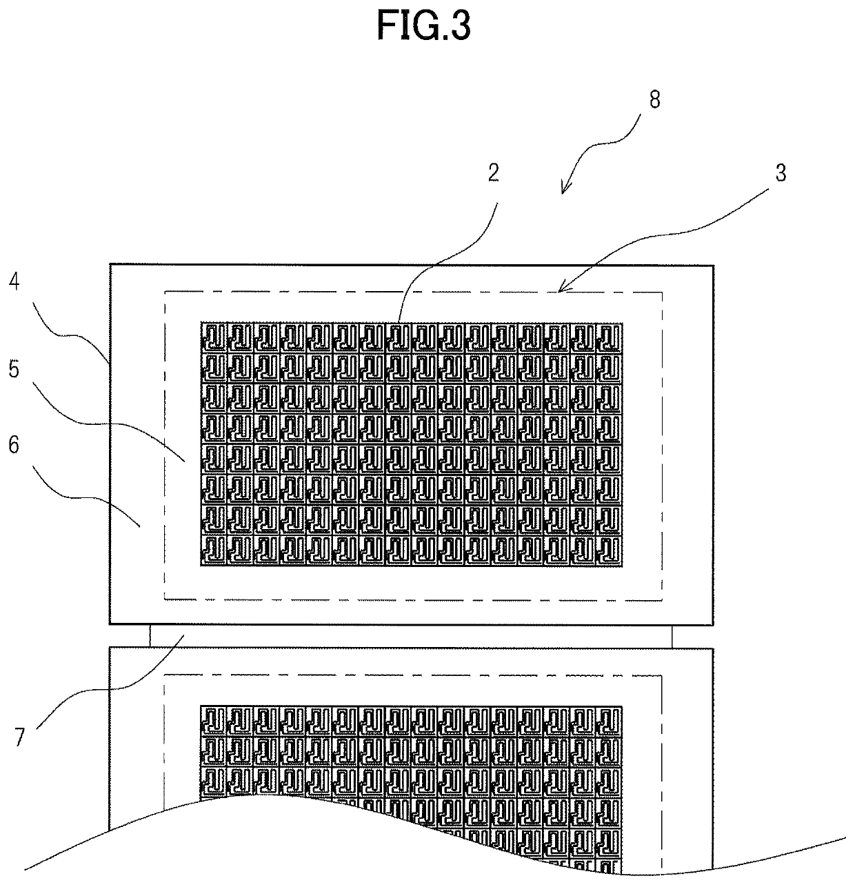
[0047]Next, a base material 8 for printed interconnect boards according to one aspect of the present invention will be described. As illustrated in FIG. 3, the base material 8 for printed interconnect boards has a large sheet shape having a plurality of products 3 and outer frame regions 4 (hereinafter, the base material 8 for printed interconnect boards may be referred to as the base material sheet 8). The base material sheet 8 includes connection regions 7 that connect the outer frame regions 4 next to each other. Because the base material 8 is formed to be substantially rectangular in a plan view, and several tens to several hundreds of interconnect board pieces 2 are disposed in one product 3, several hundreds of printed interconnect boards are manufactured at once from the base material sheet 8.

[0048](Connection Region)

[0049]A connection region 7 connects an outer frame region 4 and another outer frame region that is in communication with this outer frame region 4. That is, the...


PUM

PropertyMeasurementUnit
conductiveaaaaaaaaaa
conductive layer area rateaaaaaaaaaa
area rateaaaaaaaaaa

Abstract

A base material for printed interconnect boards according to one aspect of the present invention includes a base film; and at least one conductive layer that is layered on the base film. The base material for printed interconnect boards includes a product in which a plurality of interconnect board pieces are regularly arrayed in plan view and includes an outer frame region surrounding the product. The outer frame region includes a proximity region within 5 mm from an outer edge of the product and includes an outside region other than the proximity region. A layered conductive layer area rate of the proximity region is smaller than a layered conductive layer area rate of the product.

Description

TECHNICAL FIELD[0001]The present invention relates to a base material for printed interconnect boards and a manufacturing method of printed interconnect boards.[0002]The present application is based on and claims priority to Japanese Patent Application No. 2017-97657, filed on May 16, 2017, the entire contents of the Japanese Patent Application are hereby incorporated herein by reference.BACKGROUND ART[0003]Today, electronic devices are used in every field, and these are rapidly reduced in size. In accordance with that, printed interconnect boards used in devices are reduced in size and the interconnect density becomes remarkably dense and complex.[0004]As an efficient method of manufacturing small printed interconnect boards, a method of obtaining a large number of small printed interconnect boards from a single large base material for printed interconnect boards is known. While printed interconnect boards are reduced in size, base materials for printed interconnect boards are incr...

Claims


Application Information

Patent Timeline
Patent Type & Authority Applications(United States)
IPC IPC(8): H05K1/02H05K1/03H05K1/09H05K3/18
CPCH05K3/188H05K1/09H05K1/03H05K1/0298C25D7/00H05K3/0097H05K2203/0723H05K3/0052H05K3/108
Inventor TAKAHASHI, KENJINITTA, KOUJISAKAI, SHOICHIROMOTOMURA, JUNICHIIKEBE, MAKIMIURA, KOUSUKEITOU, MASAHIRO
Owner SUMITOMO ELECTRIC IND LTD
Features
  • R&D
  • Intellectual Property
  • Life Sciences
  • Materials
  • Tech Scout
  • Unparalleled Data Quality
  • Higher Quality Content
  • 60% Fewer Hallucinations
Learn More