Package carrier and package structure

Active Publication Date: 2020-10-15
UNIMICRON TECH CORP
View PDF0 Cites 0 Cited by
  • Summary
  • Abstract
  • Description
  • Claims
  • Application Information

AI Technical Summary

Benefits of technology

[0026]Based on the above, in the design of the package carrier of the invention, the second circuit patterns are directly connected to the first circuit patterns. In a cross-sectional view, the first thickness of each of the first circuit patterns is greater than than the second thickness of each of the second circuit patterns, and the first surface of each of the first circuit patterns is

Problems solved by technology

If the thickness of the circuit layer is greater than 70 μm, the difficulty in manufacturing either by means of electroplating or etching is increased.

Method used


Image

  • Package carrier and package structure
  • Package carrier and package structure
  • Package carrier and package structure

Examples


Embodiment Construction

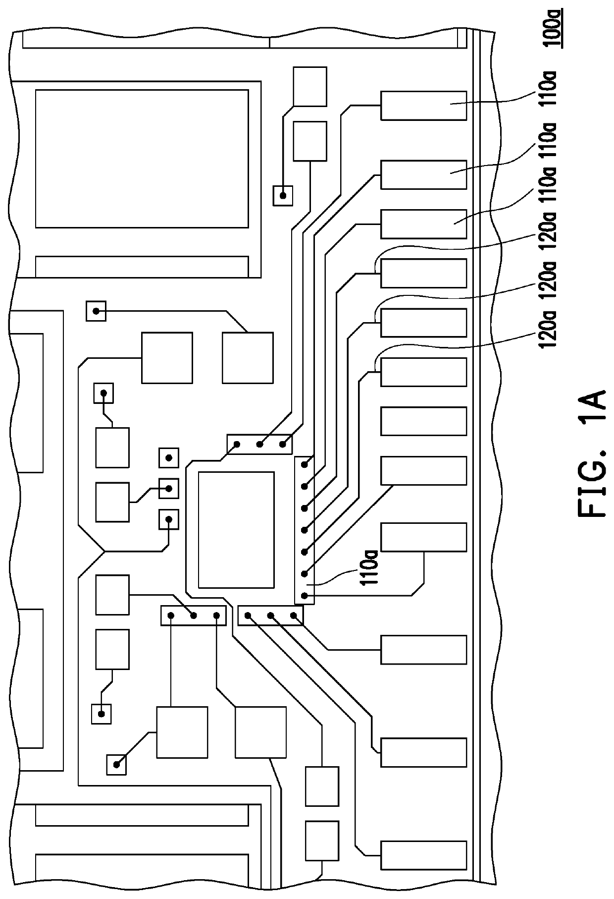
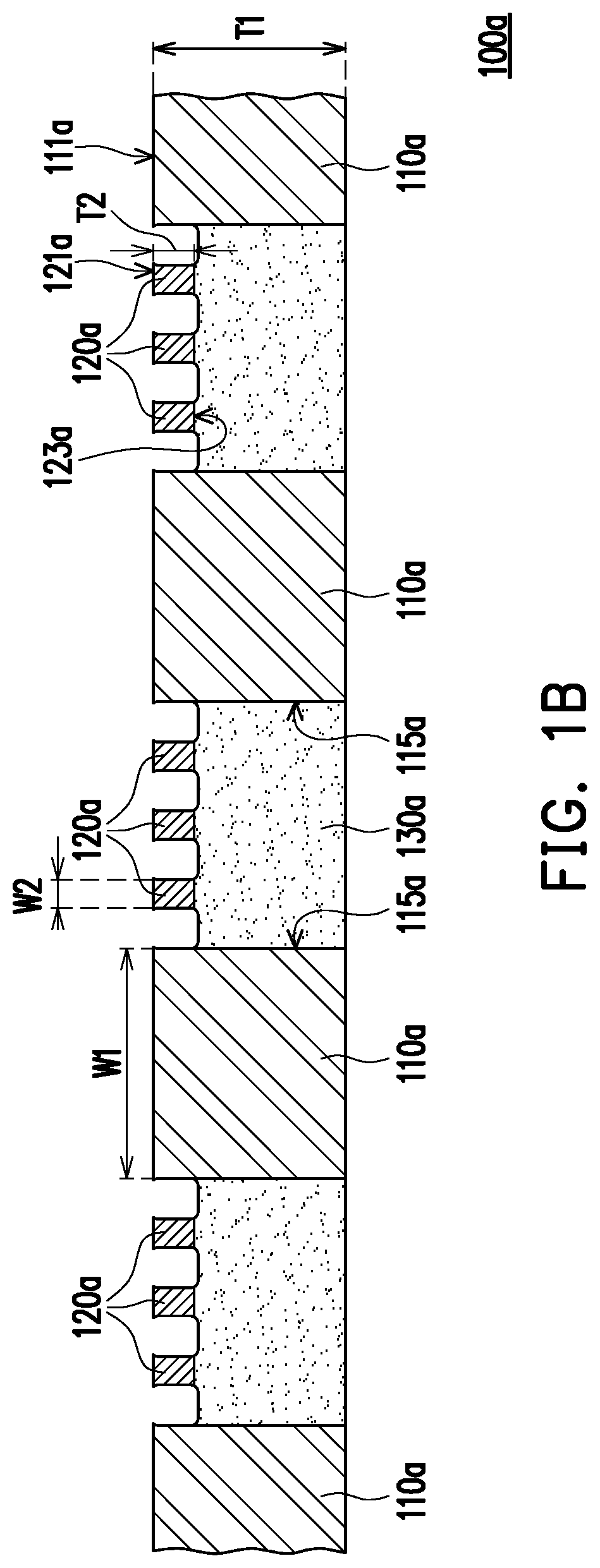
[0034]FIG. 1A is a schematic top view of a package carrier according to an embodiment of the invention. FIG. 1B is a schematic partial cross-sectional view of the package carrier depicted in FIG. 1. Referring to FIG. 1A and FIG. 1B simultaneously, in the present embodiment, a package carrier 100a includes a plurality of first circuit patterns 110a, a plurality of second circuit patterns 120a and an insulating material layer 130a. The second circuit patterns 120a are disposed between any two the first circuit patterns 110a and are directly structurally and electrically connected connected to the first circuit patterns 110a. In a cross-sectional view, a first thickness T1 of each of the first circuit patterns 110a is greater than a second thickness T2 of each of the second circuit patterns 120a. A first surface 111a of each of the first circuit patterns 110a is aligned with a second surface 121a of each of the second circuit patterns 120a. The insulating material layer 130a at least c...


PUM


Abstract

A package carrier includes a plurality of first circuit patterns, a plurality of second circuit patterns and an insulating material layer. The second circuit patterns are disposed between any two the first circuit patterns and are directly connected to the first circuit patterns. In a cross-sectional view, a first thickness of each of the first circuit patterns is greater than a second thickness of each of the second circuit patterns. A first surface of each of the first circuit patterns is aligned with a second surface of each of the second circuit patterns. The insulating material layer at least contacts the first circuit patterns.

Description

CROSS-REFERENCE TO RELATED APPLICATION[0001]This application claims the priority benefits of U.S. provisional application Ser. No. 62 / 831,738, filed on Apr. 10, 2019, and Taiwan application serial no. 108141610, filed on Nov. 15, 2019. The entirety of each of the above-mentioned patent applications is hereby incorporated by reference herein and made a part of this specification.BACKGROUNDField of the Invention[0002]The invention relates to a package carrier and a package structure and more particularly, to a package carrier including circuit patterns with two thicknesses and a package structure using the package carrier.Description of Related Art[0003]At present, a thickness of a circuit layer on a circuit carrier ranges from 180 μm to 70 μm. If the thickness of the circuit layer is greater than 70 μm, the difficulty in manufacturing either by means of electroplating or etching is increased. Moreover, a line spacing between circuits must be controlled to be much smaller than the thi...

Claims


Application Information

Patent Timeline
IPC IPC(8): H05K3/10
CPCH05K3/103H05K1/111H05K2201/0338H01L23/49811H01L23/49838H01L2224/73265H01L2224/48091H01L2924/181H05K2201/09736H05K1/0201H05K1/056H05K1/0306H05K1/0265H01L2924/00014H01L2924/00012
Inventor TAIN, RA-MINHUANG, PEI-CHANGPO, CHI-CHUNLIAO, CHUN-LINWANG, PO-HSIANGCHEN, HSUAN-WEI
Owner UNIMICRON TECH CORP
Why Eureka
Try Eureka