

Antireflection structure and manufacturing method thereof
a technology of anti-reflection structure and manufacturing method, which is applied in the direction of instruments, optical elements, vacuum evaporation coating, etc., can solve the problems of low reflection, prone to variation in the depth of the nanostructure, and difficult to produce molded products with uniform anti-reflection properties and low reflection
- Summary
- Abstract
- Description
- Claims
- Application Information
AI Technical Summary
Benefits of technology
Problems solved by technology
Method used
Image

Examples
reference example 1
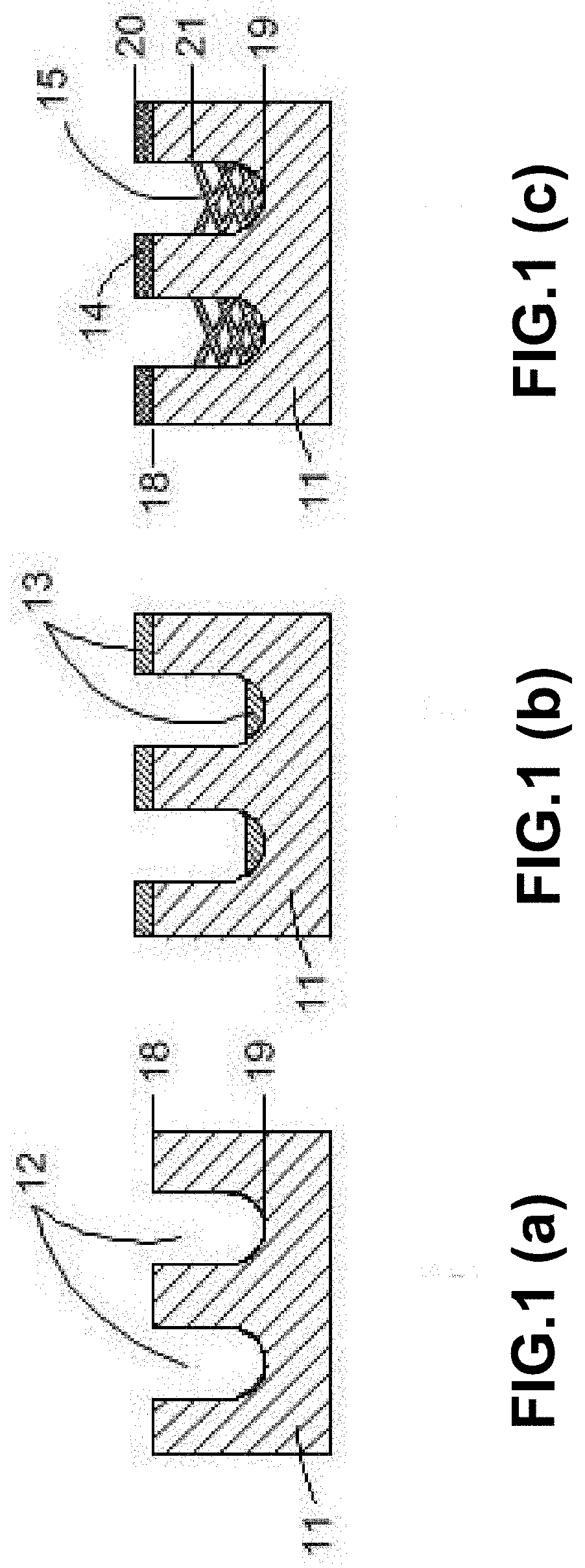
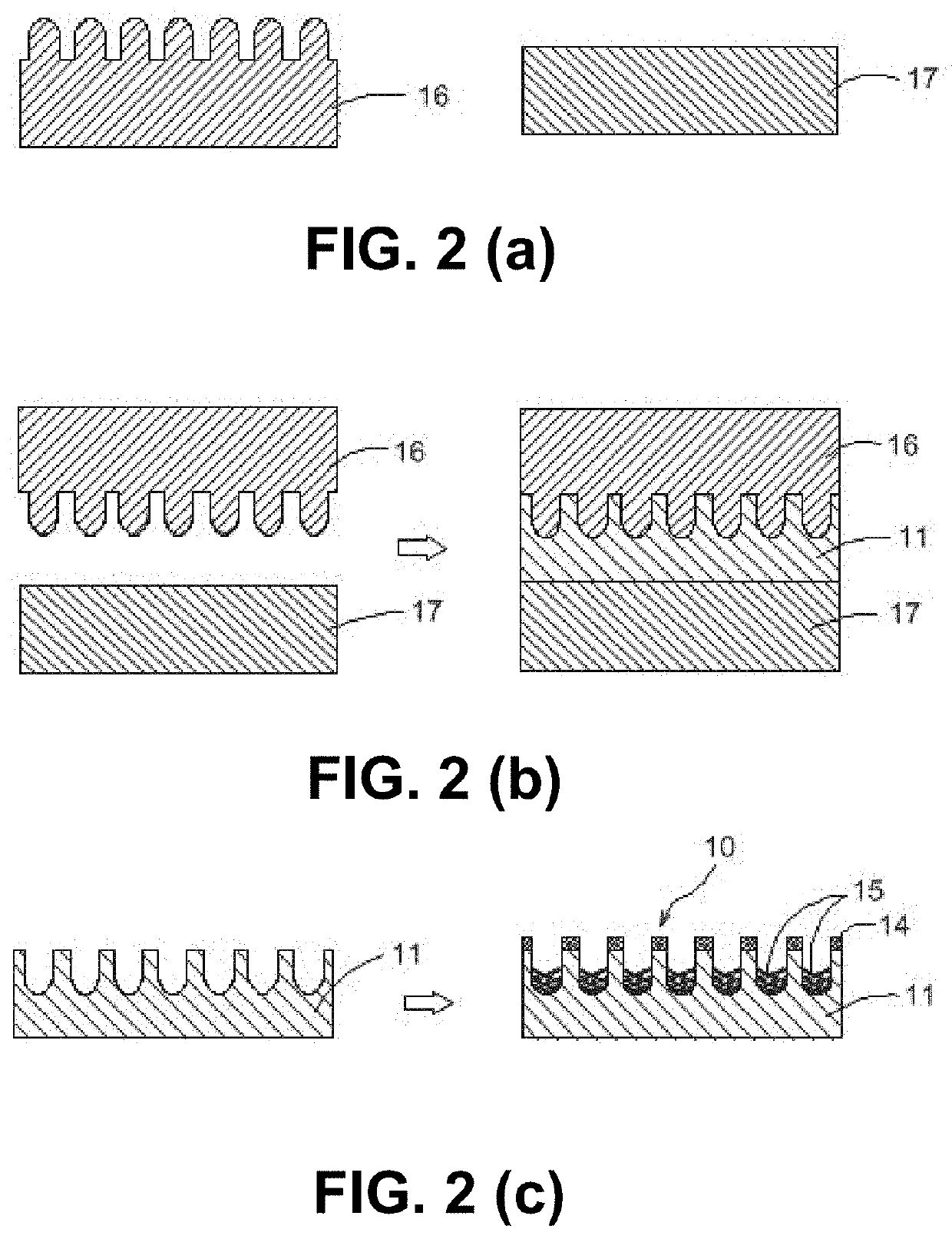
[0179]In Reference Example 1, a specimen (A) with of the U-shaped cross-sectional holes on the substrate was prepared by injection molding.
(1) Thermoplastic Resin Used for Preparing the Specimen (A)
[0180]For preparing the specimen (A), a polycarbonate resin (manufactured by
[0181]Mitsubishi Engineering Plastics Corporation, product name: Iupilone S-3000 r) was used.
(2) Preparation of Specimens (A-1 to A-3) for Evaluation
[0182]The mold used in the injection molding system was a piece mold with multiple inverted U-shaped convex cross-sectional shapes, with an average diameter of 200 nm, a height of 350 nm (in which a molding temperature is adjusted such that a depth of a molded article is 90 to 230 nm), and an average distance of 250 nm between the center points of adjacent U-shaped horizontal cross sections.
[0183]Using the above molds, several specimens (A-1), (A-2), and (A-3) were molded respectively by the injection molding method with the mold temperature set at 110° C., 120° C., a...
example 1
(1) Preparation of Specimens (B-1 to B-3) for Evaluation
[0186]The specimen (B-1), (B-2), and (B-3) in which the thin film and the columnar film of silicon oxide were formed on the surface portion and in the space portions of the holes of the above-mentioned specimens (A-1), (A-2), and (A-3) respectively were manufactured under the following condition using the above-mentioned magnetron sputtering apparatus.
(a) Target material: silicon oxide
(b) Deposition gas: A mixture of argon gas and oxygen gas (argon / oxygen molar ratio: 75 / 25)
(c) The distance between specimens (A-1 to A-3) and target: 80 mm
(d) Gas pressure: 4 Pa
(e) Sputtering time: 30 min (the time required to form a thin film with a thickness of 25 nm on the surface portion) ps (f) Specimen temperature: room temperature
(2) Evaluation Results
[0187]The above sputtering conditions and results are summarized in Table 1. For the specimen (B-2), the maximum depth was 130 nm, the minimum depth was 110 nm, and the average diameter of th...
example 2
(1) Preparation of Specimens (B-4 to B-6) for Evaluation
[0189]Using the above magnetron film sputtering apparatus, specimens (B-4), (B-5), and (B-6) were manufactured by forming thin film and columnar film of silicon oxide on the surface portion and in the space portions of the holes of the above specimens (A-1), (A-2), and (A-3), respectively, under the conditions in which the gas pressure was changed to 6 Pa, and other conditions such as the mixing ratio of gases for sputtering were the same as in Example 1.
(2) Evaluation Results
[0190]The above sputtering conditions and results are summarized in Table 1. For specimens (B-4), (B-5), and (B-6), the maximum depth, minimum depth, and average diameter of the openings were almost the same as for specimen (B-2) above.
[0191]For specimens (B-4), (B-5), and (B-6), as with specimen (B-2) above, it was determined that the silicon oxide films deposited on the surface portions were thin films with little orientation and relatively high density,...
PUM
| Property | Measurement | Unit |
|---|---|---|
| depth | aaaaa | aaaaa |
| depth | aaaaa | aaaaa |
| diameter | aaaaa | aaaaa |
Abstract
Description
Claims
Application Information