Probe structures using clamped substrates with compliant interconnectors

a technology of interconnectors and substrates, which is applied in the direction of individual semiconductor device testing, electrical apparatus construction details, instruments, etc., can solve the problems of inability to replace, multiple expensive steps in the manufacturing process used to fabricate such substrates and connect them to probe cards, and the substrates available today are problemati

Inactive Publication Date: 2005-09-20
NOVELLUS DEV
View PDF24 Cites 59 Cited by
  • Summary
  • Abstract
  • Description
  • Claims
  • Application Information

AI Technical Summary

Problems solved by technology

Substrates available today, and the manner in which they are used, are problematic for two basic reasons.
First, manufacturing techniques used to fabricate such substrates and to connect them to Probe Cards typically require multiple expensive steps.
Second, if one of the connectors on the substrate gets damaged, it cannot be replaced, for the most part, or is difficult or expensive to rework.
In addition, whenever the substrate wears out, or gets damaged, one typically has to throw away the Probe Card together with the substrate.
In particular, this is because, due to manufacturing techniques used to fabricate such substrates and to connect them to Probe Cards, it is a prohibitively lengthy and costly process to separate the substrate from the Probe Card.

Method used


Image

  • Probe structures using clamped substrates with compliant interconnectors
  • Probe structures using clamped substrates with compliant interconnectors
  • Probe structures using clamped substrates with compliant interconnectors

Examples


Embodiment Construction

[0026]As is known, circuits such as, for example and without limitation, integrated circuits (“ICs”), are fabricated on wafers, and the circuits are tested by applying electrical signals to circuit inputs and analyzing electrical signals produced at circuit outputs (such circuit inputs and outputs may be bumped or not). As is also known, a Probe Card that provides an interface between the circuit inputs and outputs (“I / O”) on the wafer and a Tester is used to perform such testing.

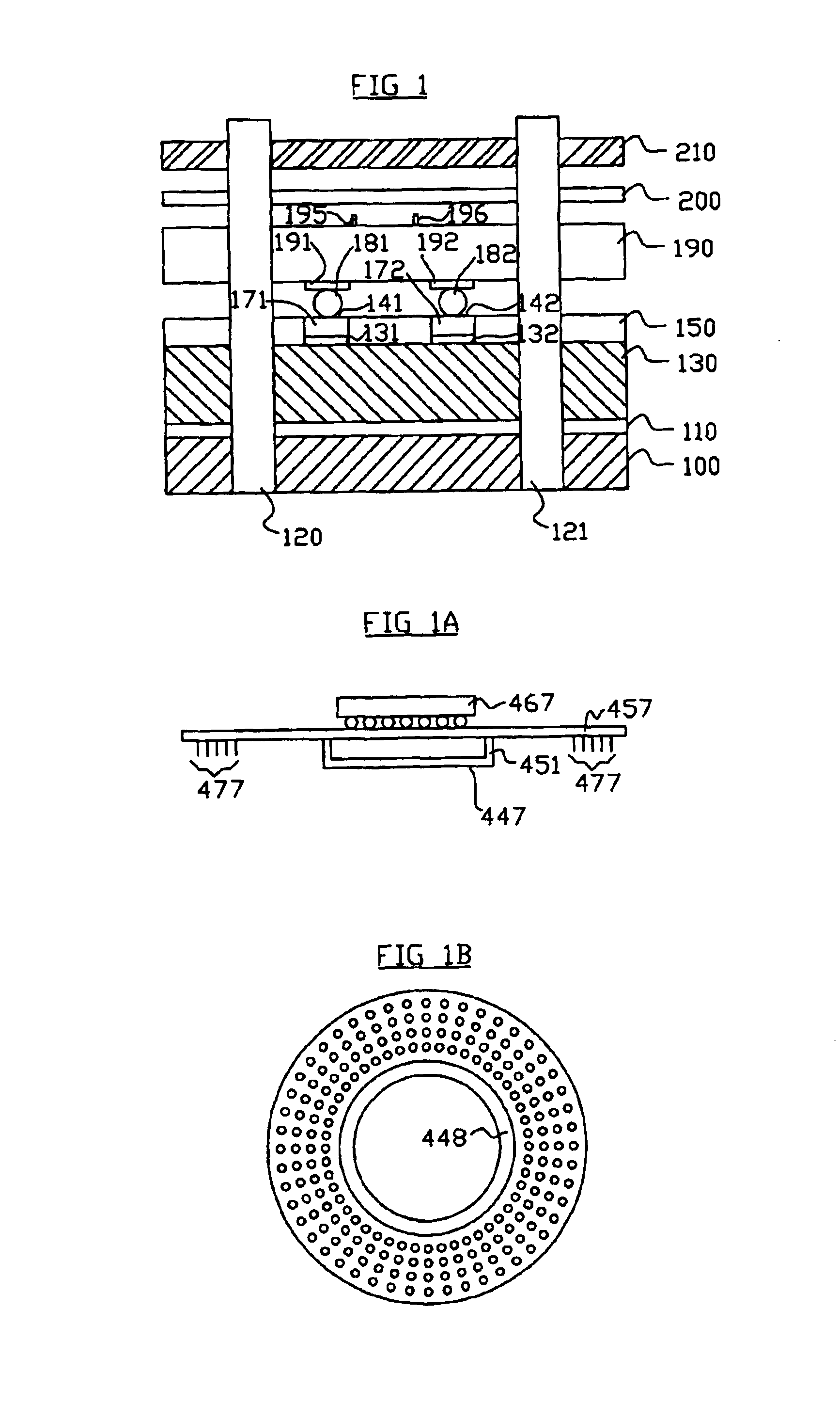
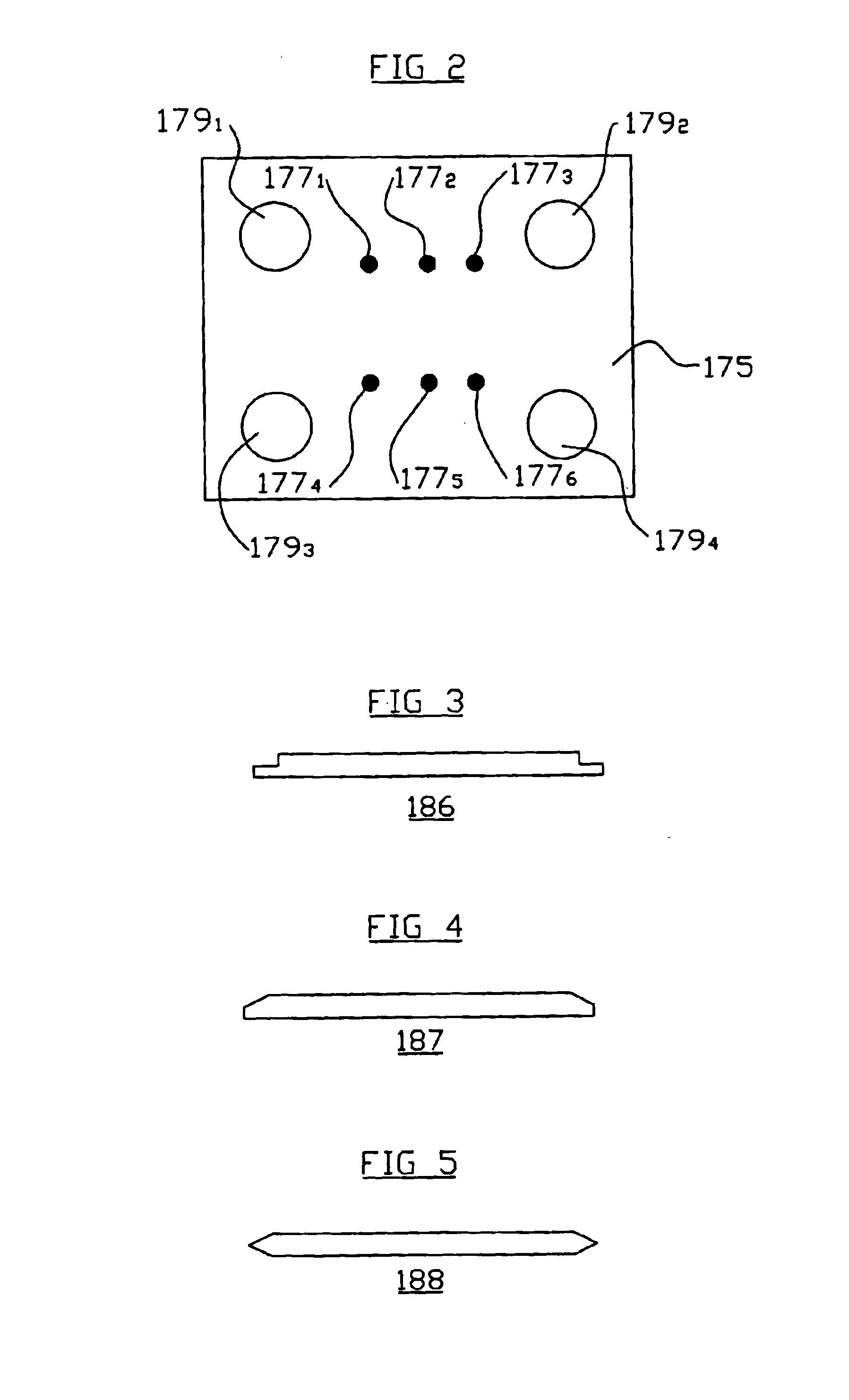
[0027]As the density of I / O of ICs has increased, it has become common to connect the Probe Card to a substrate (sometimes referred to in the art as an interposer) having an array of contactors (for example and without limitation, 12-50 μm high structures that are sometimes also referred to in the art as posts) on a top or testing side (i.e., a side that contacts the IC on the wafer) and having a ball grid array (“BGA”) of pads on a bottom side (i.e., a side that contacts the Probe Card). The contactors are...


PUM


Abstract

One embodiment of the present invention is a structure useful for testing circuits that includes: (a) a substrate having contactors on a first side and pads on a second side; (b) a card having pads on a first side; and (c) interconnectors that electrically connect the pads on the second side of the substrate with the pads on the card; wherein at least one of the interconnectors includes at least a portion that does not melt at temperatures in a range from about 183° C. to about 230° C., and the distance between the substrate and the card is determined by a dimension of the at least a portion.

Description

[0001]This is a continuation-in-part of a patent application entitled “Structures for Testing Circuits and Methods for Fabricating the Structures” having Ser. No. 10 / 387,216 which was filed on Mar. 12, 2003. This application is also related to a patent application entitled “Structures for Testing Circuits and Methods for Fabricating the Structures” having Ser. No. 10 / 386,875 which was filed on Mar. 12, 2003.TECHNICAL FIELD OF THE INVENTION[0002]One or more embodiments of the present invention pertain to: (a) one or more structures useful, for example and without limitation, for testing circuits, for example and without limitation, integrated circuits (“ICs”) at a wafer level; and (b) one or more methods for fabricating such structures.BACKGROUND OF THE INVENTION[0003]As is known, a substrate (sometimes also referred to in the art as an interposer) is a device that provides a fan-out between I / O (i.e., electrical inputs and outs) of a circuit, for example and without limitation, an i...

Claims


Application Information

Patent Timeline
Patent Type & Authority Patents(United States)
IPC IPC(8): G01R1/04G01R1/02
CPCG01R1/0483G01R31/2889G01R1/07378G01R3/00
Inventor KARAVAKIS, KONSTANTINE N.NGUYEN, TOM T.
Owner NOVELLUS DEV
Why Eureka
Try Eureka