This helps you quickly interpret patents by identifying the three key elements:
Problems solved by technology
Method used
Benefits of technology
Benefits of technology
[0012]The present invention has been made in view of the above, and an object of the present invention is therefore to provide a light emitting device in which a change of luminance of an OLED is suppressed and a desired color display can be stably performed even when an organic light emitting layer is somewhat deteriorated or when an environmental temperature is varied.
[0021]With the above-described structure, in the light emitting device of the present invention, the reduction of the luminance of the OLED can be suppressed even with the deterioration of the organic light emitting layer. As a result, a clear image can be displayed.
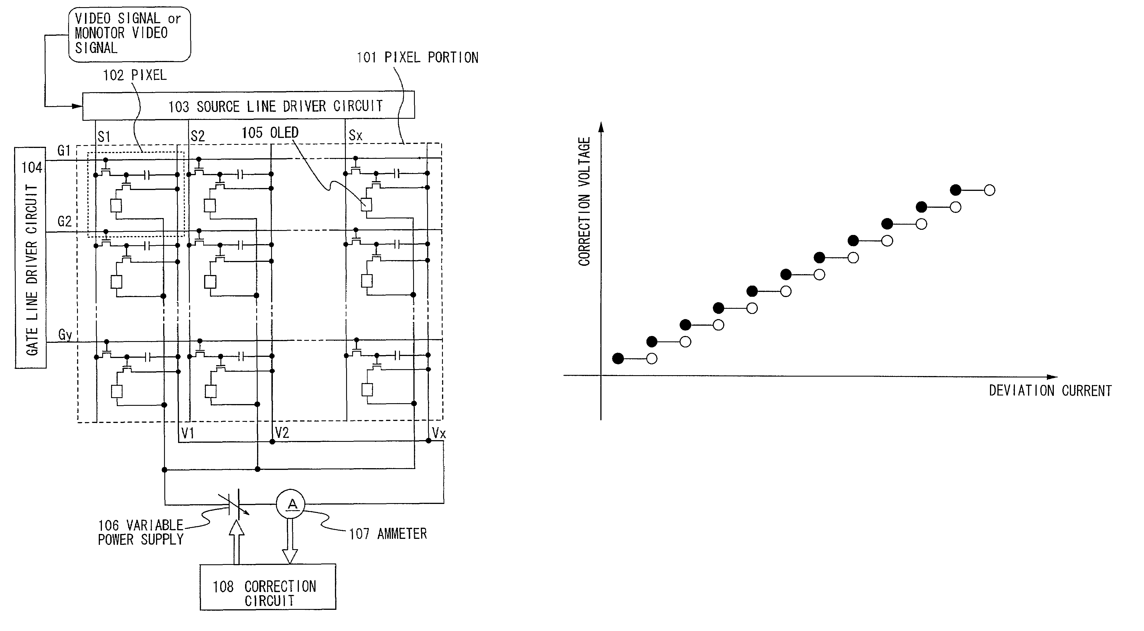
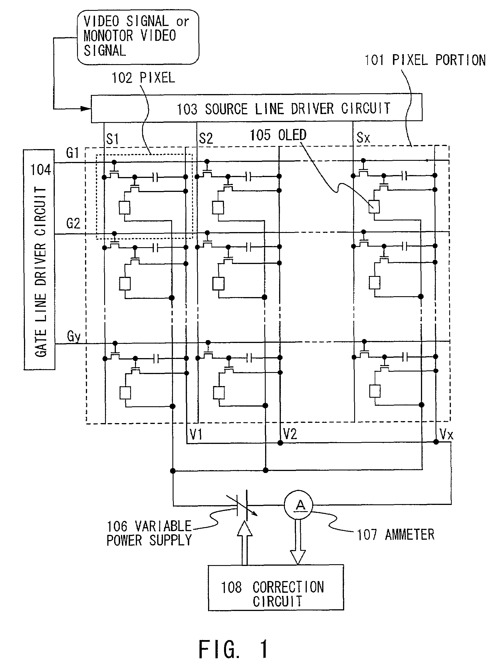
[0022]Further, in the color display mode in which three kinds of OLEDs corresponding to R (red), G (green) and B (blue) are used, monitor pixel portions corresponding to the respective colors may be provided, and the OLED driving current may be measured for every OLED of each color to thereby correct the OLED driving voltage. With this structure, the balance of luminance among the respective colors is prevented from being lost, and a desired color can be displayed even when the organic light emitting layers of the OLEDs deteriorate at different speeds in accordance with the corresponding colors.
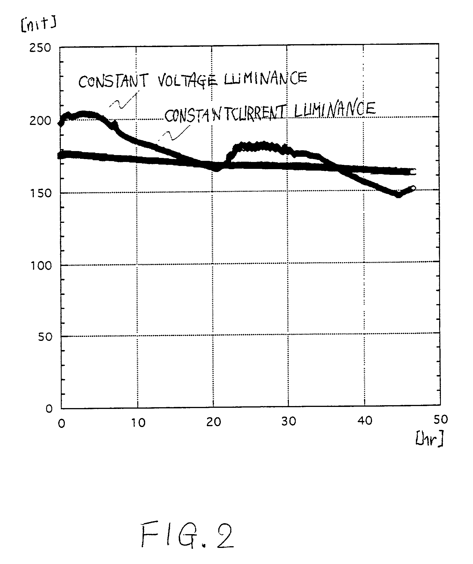
[0023]Further, a temperature of the organic light emitting layer is influenced by an outer temperature, heat generated by the OLED panel itself, or the like. Generally, when the OLED is driven at a constant voltage, the value of the flowing current changes in accordance with the temperature. FIG. 3 shows a change of a voltage-current characteristic of the OLED when the temperature of the organic light emitting layer is changed. When the voltage is constant, if the temperature of the organic light emitting layer becomes higher, the OLED driving current becomes larger. Since the relationship between the OLED driving current and the luminance of the OLED is substantially proportional, the luminance of the OLED becomes higher as the OLED driving current becomes larger. In FIG. 2, the constant voltage luminance shows a vertical period for about 24 hours. This is because a temperature difference between day and night is reflected. However, in the light emitting device of the present invention, the OLED driving current can always be kept constant by the correction of the OLED driving voltage even if the temperature of the organic light emitting layer is changed. Therefore, a constant luminance can be obtained without being influenced by the temperature change, and also, the increase in power consumption accompanied with the temperature rise can be prevented.
[0024]Moreover, a degree of the change of the OLED driving current in the temperature change generally differs depending on the kind of the organic light emitting material. Thus, in the color display, the luminances of the OLEDs of the respective colors may be separately changed in accordance with the temperature. However, in the light emitting device of the present invention, the constant luminance can be obtained without being influenced by the temperature change. Thus, the balance of luminance among the respective colors is prevented from being lost, and a desired color can be displayed.
Problems solved by technology
In putting a light emitting device to practical use, a serious problem at present is a reduction in the luminance of the OLED, which is accompanied with deterioration of the organic light emitting material contained in the organic light emitting layer.
Thus, an image having a desired color can not be displayed on the light emitting device.
Furthermore, the luminance of the OLED has large temperature depending property, and thus, there is a problem in that luminance of a display and a tone vary in accordance with the temperature in constant voltage drive.
Method used
Image
Click on the blue label to locate the original text in one second.
Reading with bidirectional positioning of images and text.
Examples
embodiment 1
[Embodiment 1]
[0069]In this embodiment, the detailed structure of a correction circuit of a light emitting device of the present invention is described.
[0070]FIG. 6 is a block diagram of the structure of the correction circuit in this embodiment. A correction circuit 203 includes an A / D converter circuit 204, a memory for measured value 205, a calculation circuit 206, a memory for reference value 207 and a controller 208.
[0071]A current value (measured value) measured with an ammeter 201 is input to the A / D converter circuit 204 of the correction circuit 203. In the A / D converter circuit 204, an analogue measured value is converted into a digital one. Digital data of the converted measured value is input to the memory for measured value 205 to be held.
[0072]On the other hand, digital data of an ideal measured value what is called a reference value is held in the memory for reference value 207. In the calculation circuit 206, the digital data of the measured value held in the memory ...
embodiment 2
[Embodiment 2]
[0077]In this embodiment, the structure of a pixel different from that in FIG. 4 in the light emitting device of the present invention is described.
[0078]FIG. 8 shows the structure of the pixel in this embodiment. In a pixel portion of the light emitting device in this embodiment, pixels 300 are provided in matrix. The pixel 300 has a source line 301, a first gate line 302 a second gate line 303, a power supply line 304, a switching TFT 305, a driving TFT 306, an erasing TFT 309 and an OLED 307.
[0079]A gate electrode of the switching TFT 305 is connected to the first gate line 302. One of a source region and a drain region of the switching TFT 305 is connected to the source line 301, and the other is connected to a gate electrode of the driving TFT 306.
[0080]A gate electrode of the erasing TFT 309 is connected to the second gate line 303. One of a source region and a drain region of the erasing TFT 309 is connected to the power supply line 304, and the other is connect...
embodiment 3
[Embodiment 3]
[0094]In this embodiment, a monitor image displayed on the pixel portion in performing correction of a current in the light emitting device of the present invention is described.
[0095]In the present invention, the correction of the current may be conducted at the time predetermined in advance by setting. Also, a user may arbitrarily determine the time of the correction.
[0096]In the case where the correction is performed at the time predetermined in advance by setting, it is preferable from the viewpoint of convenience that the image to be displayed is prevented from being changed against intention of, a user. For example, in case of a portable telephone, the setting is made such that the correction is performed only at the time when a waiting image is displayed. Also, in case of a personal computer (PC), the setting is made such that the correction is performed only at the time while a screen-saver for preventing a screen from burning is being started. A reference valu...
PUM
Abstract
A light emitting device with a simple and easy structure without waste is provided, in which a change of luminance of an OLED is suppressed and a desired color display can be stably performed even if an organic light emitting layer is somewhat deteriorated or an environmental temperature is varied. A driving current of the OLED of a pixel portion is measured, and a value of the voltage supplied to the pixel portion from a variable power supply is corrected such that the measured driving current has a reference value. When the driving current of the OLED is measured, a monitor video signal of a different system from that of a video signal for displaying an image is used to display a monitor image on the pixel portion. With the above-described structure, a reduction of the luminance accompanied with the deterioration of the organic light emitting layer can be suppressed. As a result, a clear image can be displayed.
Description
BACKGROUND OF THE INVENTION[0001]1. Field of the Invention[0002]The present invention relates to an OLED panel in which an organic light emitting device (OLED) formed on a substrate is enclosed between the substrate and a cover member. Also, the present invention relates to an OLED module in which a controller IC or the like is mounted on the OLED panel. Note that, in this specification, the OLED panel and the OLED module are generically called light emitting devices. The present invention further relates to an electronic device using the light emitting device.[0003]2. Description of the Related Art[0004]An OLED emits light by itself, and thus, has high visibility. The OLED does not need a backlight necessary for a liquid crystaldisplay device (LCD), which is suitable for a reduction of a light emitting device in thickness. Also, the OLED has no limitation on a viewing angle. Therefore, the light emitting device using the OLED has recently been attracting attention as a display dev...
Claims
Application Information
Patent Timeline
Application Date:The date an application was filed.
Publication Date:The date a patent or application was officially published.
First Publication Date:The earliest publication date of a patent with the same application number.
Issue Date:Publication date of the patent grant document.
PCT Entry Date:The Entry date of PCT National Phase.
Estimated Expiry Date:The statutory expiry date of a patent right according to the Patent Law, and it is the longest term of protection that the patent right can achieve without the termination of the patent right due to other reasons(Term extension factor has been taken into account ).
Invalid Date:Actual expiry date is based on effective date or publication date of legal transaction data of invalid patent.

