Check patentability & draft patents in minutes with Patsnap Eureka AI!

Dynamic semiconductor memory device and power saving mode of operation method of the same

a technology of dynamic semiconductor and memory device, which is applied in the direction of information storage, static storage, digital storage, etc., can solve the problems of high power consumption, battery cannot be used for a long time period, and data “high” stored in the capacitor is lost, and achieves the effect of low power consumption

Inactive Publication Date: 2007-01-23
SAMSUNG ELECTRONICS CO LTD
View PDF9 Cites 1 Cited by
  • Summary
  • Abstract
  • Description
  • Claims
  • Application Information

AI Technical Summary

Benefits of technology

This approach doubles the refresh cycle period, halves the refresh time, and decreases power consumption by a factor of 4 to 16, making it suitable for use in mobile communication terminals by reducing battery drain.

Problems solved by technology

A data “high” stored in the capacitor is lost as time lapses.
A conventional dynamic semiconductor memory device should perform a periodic refresh operation even in a standby state, when write and read operations are not performed, leading to high power consumption.
When the conventional dynamic semiconductor memory device is used in a mobile communication terminal that uses a battery as a power source, the battery cannot be used for a long time periods because the refresh operation has such a high power consumption.

Method used


Image

  • Dynamic semiconductor memory device and power saving mode of operation method of the same
  • Dynamic semiconductor memory device and power saving mode of operation method of the same
  • Dynamic semiconductor memory device and power saving mode of operation method of the same

Examples


Embodiment Construction

[0020]The present invention will now be described more fully with reference to the accompanying drawings, in which preferred embodiments of the invention are shown. This invention may, however, be embodied in different forms and should not be construed as limited to the embodiments set forth here. Rather, these embodiments are provided so this disclosure will be thorough and complete, and will fully convey the scope of the invention to those skilled in the art. Like numbers refer to like elements throughout the specification.

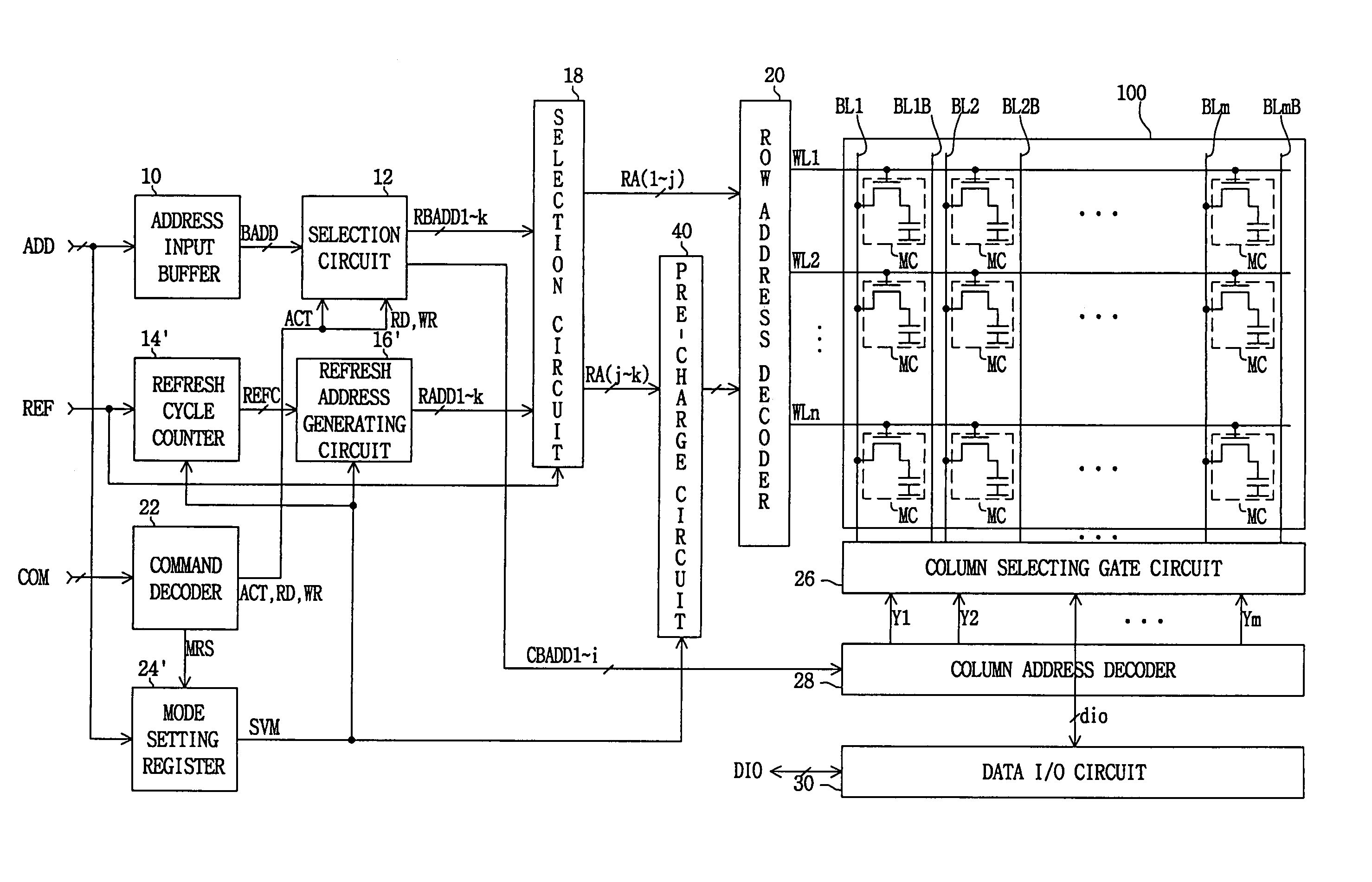
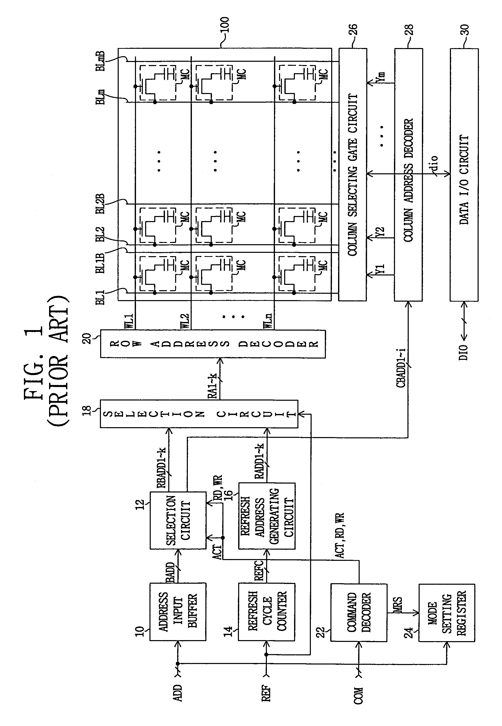
[0021]FIG. 1 is a block diagram of a conventional dynamic semiconductor memory device. The dynamic semiconductor memory device of FIG. 1 includes an address input buffer 10, selection circuits 12 and 18, a refresh cycle counter 14, a refresh address generating circuit 16, a row address decoder 20, a command decoder 22, a mode setting register 24, a column selecting gate circuit 26, a column address decoder 28, a data I / O circuit 30, and a memory cell array 100.

[...


PUM


Abstract

A dynamic semiconductor memory device includes a memory cell array including a plurality of memory cells connected between a plurality of word lines and a plurality of bit line pairs. A mode setting portion receives a mode setting code applied from an external portion to generate a power saving mode control signal for a power saving mode of operation responsive to a mode setting command. An address control portion decodes an address applied from an external portion or a refresh address to select one of the plurality of the word lines during a normal mode operation. The address control portion also selects a predetermined number of bits of the address during a power saving mode of operation. The semiconductor memory device, therefore extends the refresh cycle while reducing the refresh time resulting in a lower power consumption.

Description

CROSS-REFERENCE TO RELATED APPLICATION[0001]This application claims priority from Korean Patent Application No. 2003-101575, filed Dec. 31, 2003, the disclosure of which is incorporated by reference in its entirety.BACKGROUND OF THE INVENTION[0002]1. Field of the Invention[0003]The present invention relates to a dynamic semiconductor memory device and, more particularly, to a dynamic semiconductor memory device that reduces power consumption and an associated method for reducing power consumption.[0004]2. Description of the Related Art[0005]A dynamic semiconductor memory device performs refresh and read and write operations.[0006]A dynamic cell of the dynamic semiconductor memory device includes one transistor and one capacitor to store a 1-bit data. A data “high” stored in the capacitor is lost as time lapses. A refresh operation is periodically performed to maintain the data before the data “high” is lost.[0007]A conventional dynamic semiconductor memory device should perform a pe...

Claims


Application Information

Patent Timeline
Patent Type & Authority Patents(United States)
IPC IPC(8): G11C7/00G11C5/00G11C8/08G11C8/18G11C11/406G11C11/408
CPCG11C8/08G11C8/18G11C11/4087G11C11/406G11C2211/4067
Inventor KYUNG, KYE-HYUNHAN, KYU-HAN
Owner SAMSUNG ELECTRONICS CO LTD
Features
  • R&D
  • Intellectual Property
  • Life Sciences
  • Materials
  • Tech Scout
  • Unparalleled Data Quality
  • Higher Quality Content
  • 60% Fewer Hallucinations
Learn More