Self-calibrating anti-blooming circuit for CMOS image sensor having a spillover protection performance in response to a spillover condition

a self-calibrating, image sensor technology, applied in the field of self-calibrating anti-blooming circuit for cmos image sensor, can solve the problems of limited dynamic range and blooming, cmos image sensor suffers, and the effective dynamic range of the imager is reduced, and the resulting image is shortened. , the effect of reducing the effective dynamic rang

Inactive Publication Date: 2008-06-03
RE SECURED NETWORKS LLC
View PDF3 Cites 131 Cited by
  • Summary
  • Abstract
  • Description
  • Claims
  • Application Information

AI Technical Summary

Benefits of technology

[0047]Thus, if an anti-blooming circuit removes electrons from the well before it is full, it can reduce the effective dynamic range of the imager and decrease the fidelity of the resulting image to the true scene. Dynamic range is the ratio of the highest (lightest) signal than an imager can record to the lowest (darkest) signal. The lightest signal would correspond to the brightest highlights in an image, the darkest signal to the deepest shadows. In order to best use the dynamic range of an imager, a brighter image may call for shorter integration times and a darker image may call for longer integration times.

Problems solved by technology

Conventionally, CMOS image sensors have several limitations, for example, limited dynamic range and blooming.
A problem from which conventional CMOS image sensors suffer is a phenomenon called blooming.
Image sensor devices that integrate charge created by incident photons have dynamic range limited by the amount of charge that can be collected and held in a given photosite.
Blooming is a phenomenon in which excess charge from a pixel spills over into adjacent pixels, causing blurring and related image artifacts.
Another problem conventional CMOS image sensors have is limited dynamic range.
This can be problematic for imaging large dynamic range scenes, such as outdoor scenes.
This means that even before the pixel is completely full, the output of the pixel loses gain and the dynamic range of the pixel circuit is limited.
The problems of blooming and limited dynamic range are related.
If the reset voltage is too low, no electrons (or an insufficient number of electrons) will be shunted out of the pixel well and blooming may occur.
If the reset voltage is too high, blooming will be prevented, but at the cost of limiting the dynamic range of the pixel, because electrons will be shunted out of the pixel well before the well is full, limiting the maximum charge that can be collected.
Prior approaches to biasing the reset transistor that used a fixed bias voltage failed to account for these variations, and suffered from blooming or reduced dynamic range.

Method used


Image

  • Self-calibrating anti-blooming circuit for CMOS image sensor having a spillover protection performance in response to a spillover condition
  • Self-calibrating anti-blooming circuit for CMOS image sensor having a spillover protection performance in response to a spillover condition
  • Self-calibrating anti-blooming circuit for CMOS image sensor having a spillover protection performance in response to a spillover condition

Examples


Embodiment Construction

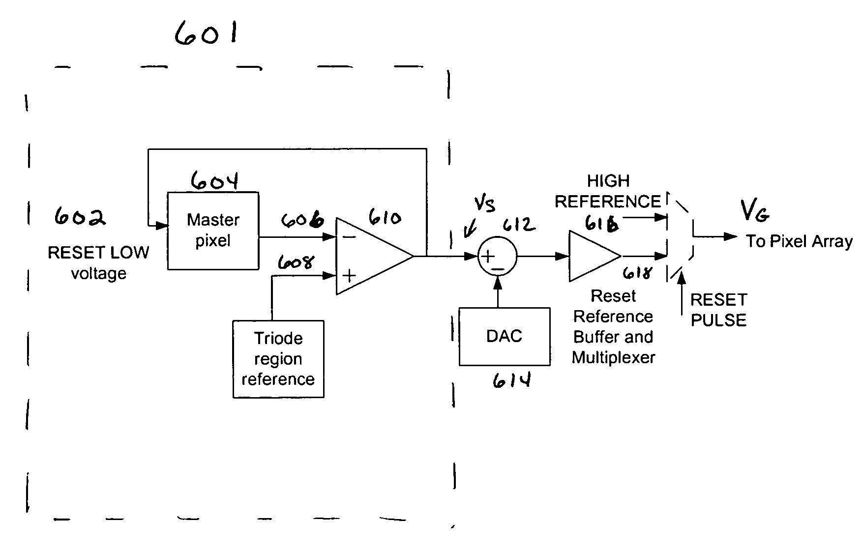
[0034]Embodiments of the invention provide a method and an apparatus for providing blooming protection for a imager cell, or a pixel, in an image array while extending the dynamic range. The terms imager cell, pixel cell and pixel may be used interchangeably in this description. Also, the terms imager array and pixel array may be used interchangeably in this description. Each pixel in an image array may include at least one transistor for resetting the pixel, typically an n-channel, metal-oxide-semiconductor field-effect transistor (MOSFET). The reset transistor receives a voltage at its gate terminal. The gate voltage, in turn, controls whether the reset transistor will operate to reset the pixel well or as an anti-blooming drain.

[0035]Embodiments of the invention provide a method and an apparatus to determine the voltage VG applied to the reset transistor to prevent blooming without sacrificing dynamic range, by taking into account the manufacturing process parameters and temperat...


PUM


Abstract

A method and apparatus to provide blooming protection for a pixel in an array while extending dynamic range.

Description

BACKGROUND OF THE INVENTION[0001]1. Technical Field[0002]The invention is related to semiconductor imaging devices and in particular to such a device that can be fabricated using a standard CMOS process. The present invention provides a method and an apparatus to providing blooming protection for a pixel in an array while extending dynamic range.[0003]2. Background Art[0004]A complementary metal-oxide semiconductor (CMOS) image sensor is a device for converting optical images to electrical signals. That is, it responds to the visible light, and the signal electrons thus formed are converted to voltages. Then the voltages are subjected to a signal processing to reconvert the voltages to image information.[0005]To provide context for the invention, an exemplary CMOS imaging system is described below. FIG. 1 is a block diagram of an imaging system 100 including an image capture circuit 110, a control circuit 112, an image processor 114 and an output device 116 all intercoupled as depic...

Claims


Application Information

Patent Timeline
Patent Type & Authority Patents(United States)
IPC IPC(8): H01L27/00H04N5/353H04N5/359H04N5/374
CPCH04N5/235H04N5/355H04N5/3592H04N23/70H04N25/57H04N25/622
Inventor TAN, MEHMET ALILUO, JIAFU
Owner RE SECURED NETWORKS LLC
Why Eureka
Try Eureka