Method and device for dividing plate-like member

a technology of a platelike member and a dividing device, which is applied in the direction of metal working equipment, manufacturing tools, welding/soldering/cutting articles, etc., can solve the problems of increasing the cost of consumables, forming parts which are not divided, and affecting the quality of the product, so as to achieve the effect of improving productivity, running cost and quality

Inactive Publication Date: 2008-08-12
TOKYO SEIMITSU
View PDF11 Cites 6 Cited by
  • Summary
  • Abstract
  • Description
  • Claims
  • Application Information

AI Technical Summary

Benefits of technology

[0018]According to the present invention, the tape is irradiated with UV rays (light in the wavelength region of ultraviolet rays) during expanding. By irradiation with UV rays, it is possible to cure an adhesive of the tape and to change the adhesion of the tape and, therefore, the elongation of the tape can be made uniform all over the surface of the plate-like member when the tape is elongated by applying a tension thereto. As a result, it is possible to positively manufacture an ultrathin chip with a good end-face shape in which uncut portions, chipping and breakage do not occur when multiple substrates are obtained by dividing the plate-like member along the linear modified region.
[0019]Also, according to the present invention, it is necessary only that UV ray irradiation means be added to a conventional device for dividing a plate-like member, and the construction of the apparatus can be made simple. The dividing work of a plate-like member becomes also simple. As a result, it becomes possible to miniaturize the apparatus for dividing a plate-like member and the dividing work of a plate-like member can be performed in a short time.
[0021]In the present invention, it is preferred that in the expanding step, the tape be irradiated with UV rays in a pattern by use of a photomask. This is because if the tape is irradiated with UV rays in a pattern like this, by discriminating between the tape in a portion corresponding to the linear modified region of the plate-like member and the tape in other portions, the adhesion of the tape is changed and the cured condition of the adhesive of the tape is changed, whereby the area near the modified region of the plate-like member is selectively expanded and the expanding force of the tape can be efficiently transmitted as a dividing force to the plate-like member, with the result that the object of the present invention that an ultrathin substrate with a good end-face shape is positively manufactured is more easily achieved. Incidentally, in the present invention, a “pattern” refers to a specific pattern which is made on the basis of the size and shape of individual substrates obtained by the dividing of the plate-like member, and an aggregate or array of the specific pattern and which is used to selectively irradiate the tape with UV rays.

Problems solved by technology

However, in such conventional methods for dividing a plate-like member, it was necessary to use a protective tape for preventing the pollution of a wafer surface during the grinding of the back surface of the wafer and a dicing tape for holding chips after dicing and this lead to an increase in the cost of consumables.
Furthermore, in the case of an ultrathin wafer having a thickness of not more than 100 μm, under conventional methods by which a wafer is cut by use of a dicing saw, chipping and breakage are formed during cutting, thereby posing the problem that good chips become defective products.
However, in the techniques proposed in the above-cited unexamined patent publications, a dicing device by a dividing technique by use of laser beams is proposed in place of a conventional dicing device by a dicing saw, and although the problem that chippings and breakage occur in a wafer during cutting is solved, the problem that in the expanding step, portions which are not divided are formed and end-face shapes of divided chips become poor.
In conventional methods and apparatus for dividing a plate-like member, however, it is often that in the expanding step, the elongation of the dicing tape S does not become uniform all over the surface of the wafer W. For example, the dicing tape S in a portion where cutting has already been performed is locally elongated, and it becomes impossible to apply a tension to the dicing tape S in uncut portions.
As a result, it is often that uncut portions are formed and that the end-face shapes of divided chips do not become linear and become poor.

Method used


Image

  • Method and device for dividing plate-like member
  • Method and device for dividing plate-like member
  • Method and device for dividing plate-like member

Examples


first embodiment

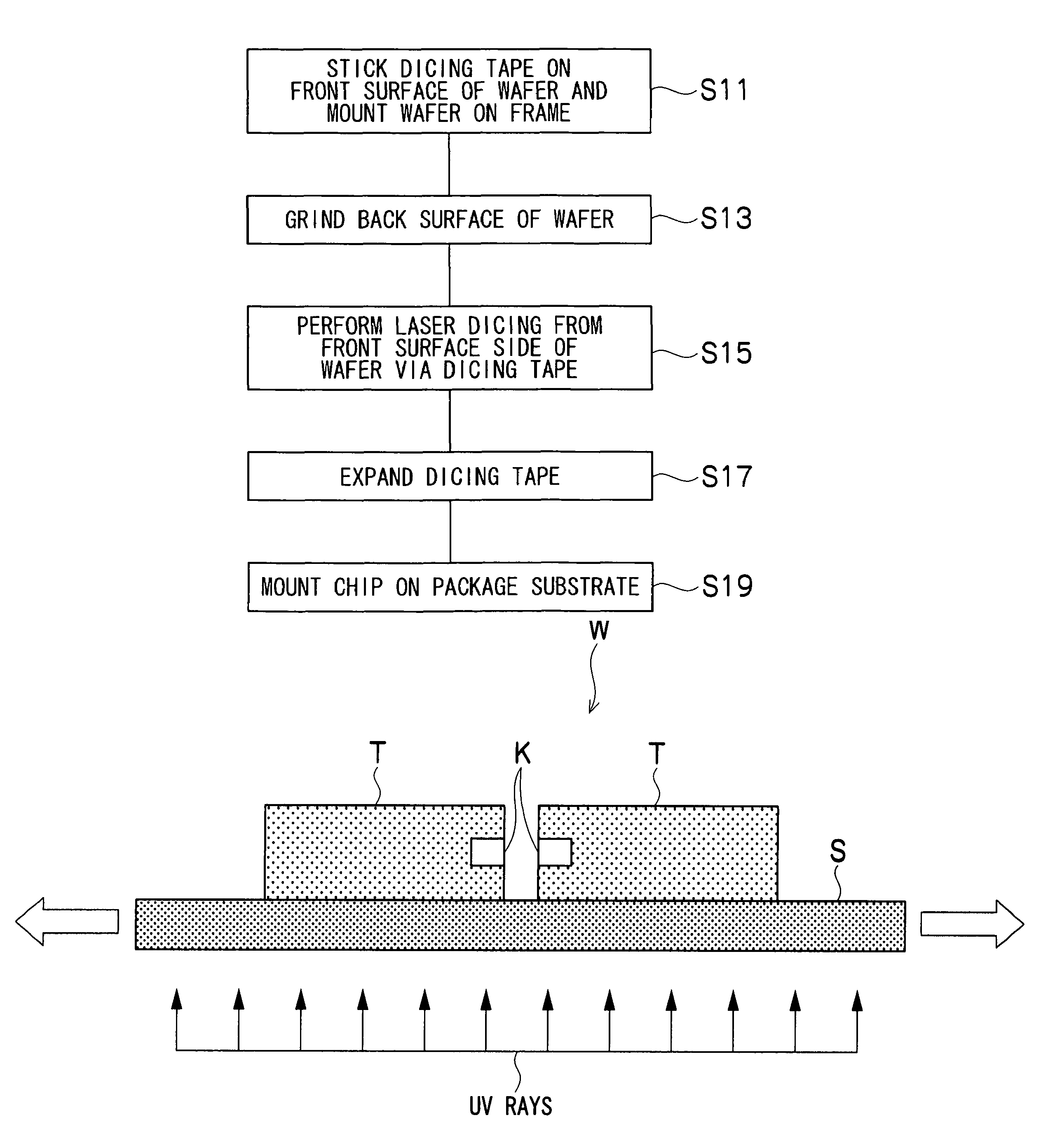
[0041]Subsequently, one chip in an expanded condition is pushed up from the dicing tape side and exfoliated from the dicing tape, this chip is sucked by a pickup head and sucked by a collet for chip mounting, with the front and back surfaces reversed, and the chip is mounted on a package substrate, such as a lead frame (Step S19). After the chip mounting step, the packaging step of wire bonding, molding, lead trimming and forming, marking, etc. is performed and an IC is completed. The foregoing is an outline of the

[0042]Next, details of the expanding step will be given. FIG. 3 is a conceptual diagram to explain the principle of a method for dividing a plate-like member related to the present invention, and FIG. 4 is a sectional view which shows an outline of the first embodiment.

[0043]As shown in FIG. 3, a modified region K formed by laser beams is present in the interior of a wafer W. As shown in FIG. 3, the tension applied to the wafer W on both sides of the modified region K via ...

second embodiment

[0057]According to the above-described second embodiment, in the expanding step, due to the irradiation with the UV rays through the photomask M, the adhesion of the dicing tape S can be selectively reduced in the irradiated portion 30 and the expanding force of the dicing tape S can be efficiently transmitted as a dividing force to the wafer W all over the surface of the wafer W. As a result of this, it is possible to manufacture an ultrathin chip with a good end-face shape in which uncut portions, chipping and breakage do not occur when chips T are obtained by dividing the wafer W along the linear modified region K.

[0058]Incidentally, in the second embodiment, it is also possible to use a dicing tape S of high adhesion.

[0059]Next, the third embodiment related to the present invention will be described on the basis of FIG. 6. This third embodiment differs from the above-described first and second embodiments only in the expanding step. Therefore, detailed descriptions of other comm...


PUM

PropertyMeasurementUnit
thicknessaaaaaaaaaa
thicknessaaaaaaaaaa
thicknessaaaaaaaaaa

Abstract

In a method and an apparatus for dividing a plate-like member related to the present invention, multiple substrates are obtained by forming a linear modified region on a surface of a plate-like member formed from a hard and brittle material or in the interior of the plate-like member and dividing the plate-like member along this modified region. The method for dividing a plate-like member includes a tape sticking step which involves sticking tape on the surface of the plate-like member, a modified region forming step which involves forming a modified region on surface of the plate-like member or in the interior of the plate-like member, and an expanding step which involves elongating the tape by applying a tension thereto after the modified region forming step. In the expanding step, the tape is irradiated with UV rays. As a result of this, it is possible to positively manufacture an ultrathin chip with a good end-face shape in which uncut portions, chipping and breakage do not occur.

Description

TECHNICAL FIELD[0001]The present invention relates to a method and an apparatus for dividing a plate-like member from which chips for semiconductor devices, electronic parts and the like are manufactured and, more particularly, to a method and an apparatus for dividing a plate-like member which are suitable for working a wafer to a prescribed thickness by grinding the back surface of the wafer and thereafter performing working for forming a modified region by laser beams and dividing the wafer into individual chips.BACKGROUND ART[0002]In recent years, ultrathin IC chips which are built in ultrathin IC cards and the like represented by a smart card have been required. Such ultrathin IC chips are manufactured by dividing an ultrathin wafer of not more than 100 μm into individual chips.[0003]Against this background, in conventional methods for dividing a plate-like member for semiconductor devices, electronic parts and the like, as shown in the flowchart of FIG. 7, a protective tape st...

Claims


Application Information

Patent Timeline
Patent Type & Authority Patents(United States)
IPC IPC(8): H01L21/50H01L21/301H01L21/44H01L21/46H01L21/78H01L21/48B23K26/00B23K26/40B28D5/00H01L21/00
CPCB23K26/4075B23K26/0057B28D5/0052H01L21/67132B28D5/0011B23K2201/40B23K26/40B23K26/53B23K2101/40B23K2103/50H01L21/78
Inventor SAKAYA, YASUYUKIAZUMA, MASAYUKI
Owner TOKYO SEIMITSU
Why Eureka
Try Eureka