Contact image sensor module and image reading device equipped with the same

a technology of image sensor and reading device, which is applied in the field of contact image sensor module and image reading device equipped with the same, can solve the problems of large noise generated in image sensor, high manufacturing cost, and inability to read clearly originals that are positioned at a position away from the platen surface of original plates, and achieve high reading speed and high image quality.

Inactive Publication Date: 2008-12-30
SEIKO EPSON CORP
View PDF13 Cites 57 Cited by
  • Summary
  • Abstract
  • Description
  • Claims
  • Application Information

AI Technical Summary

Benefits of technology

[0011]The present invention has been made in view of the above problems. A first object of the invention is to provide a contact image sensor module that can clearly read both originals positioned on a platen surface of an original platen of an image reading device and originals positioned away from the platen surface. A second object of the invention is to provide an image reading device equipped with contact image sensor module that can clearly read both originals positioned on a platen surface of an original platen of the image reading device and originals positioned away from the platen surface. A third object of the invention is to provide an image reading device equipped with contact image sensor module, which is high in reading speed and can read images of high image quality.

Problems solved by technology

However, since a contact image sensor module is shallow in the depth of field, an original that is positioned at a position away from a platen surface of an original platen cannot be read clearly.
However, the image reading devices described Patent Documents 2 and 3 are complex in the arrangement of the optical system, long in optical path, and thus high in manufacturing cost and not suited for compact size.
In general, the higher the resolution of an image sensor, the greater the noise generated in the image sensor.
The image reading device described in Patent Document 1 is thus slow in reading speed.
However, the image reading devices described Patent Documents 2 and 3 are complex in the arrangement of the optical system, long in optical path, and thus high in manufacturing cost and not suited for compact size.Patent Document 1: Japanese Unexamined Patent Publication No. 2001-133906Patent Document 2: Japanese Unexamined Patent Publication No. 2003-37712Patent Document 3: Japanese Unexamined Patent Publication No. 2003-37713

Method used


Image

  • Contact image sensor module and image reading device equipped with the same
  • Contact image sensor module and image reading device equipped with the same
  • Contact image sensor module and image reading device equipped with the same

Examples


first embodiment

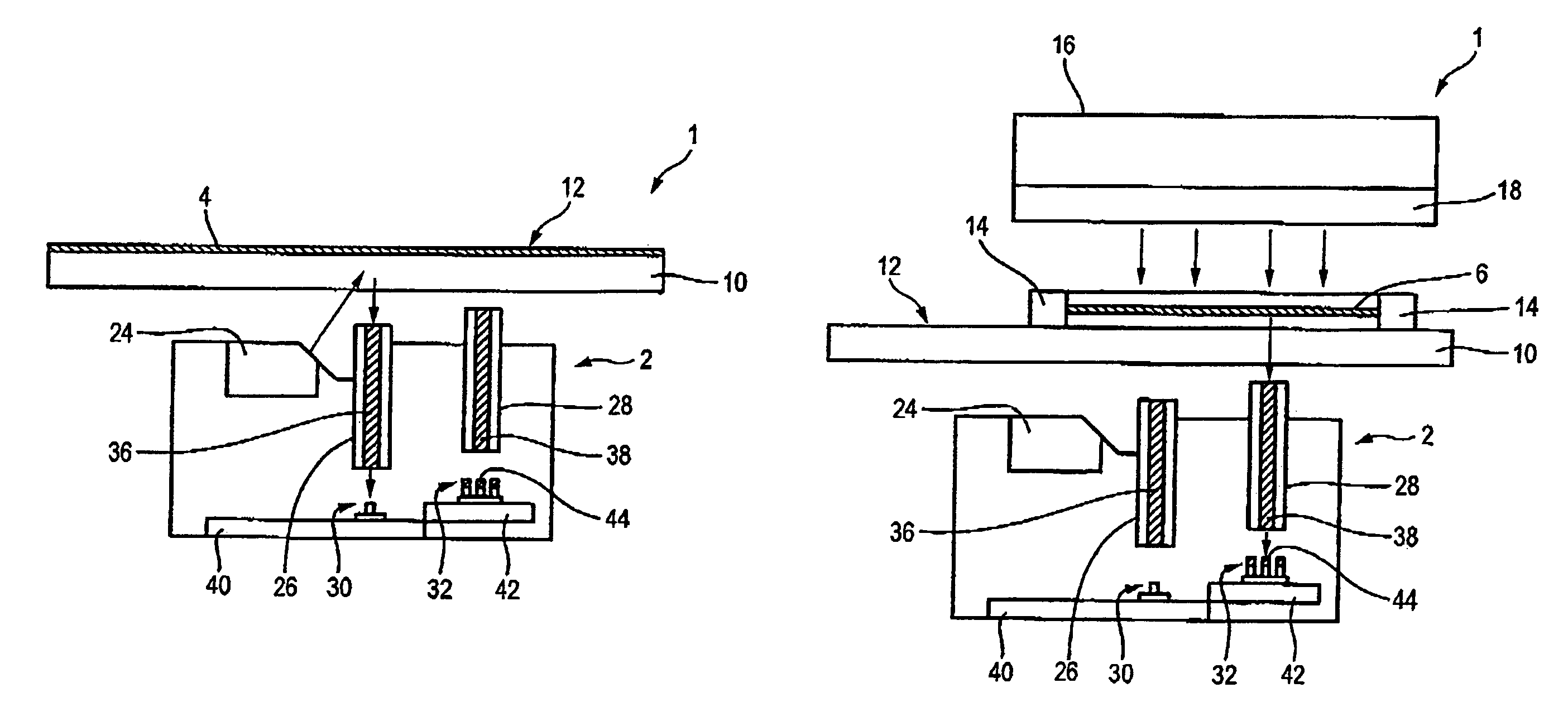
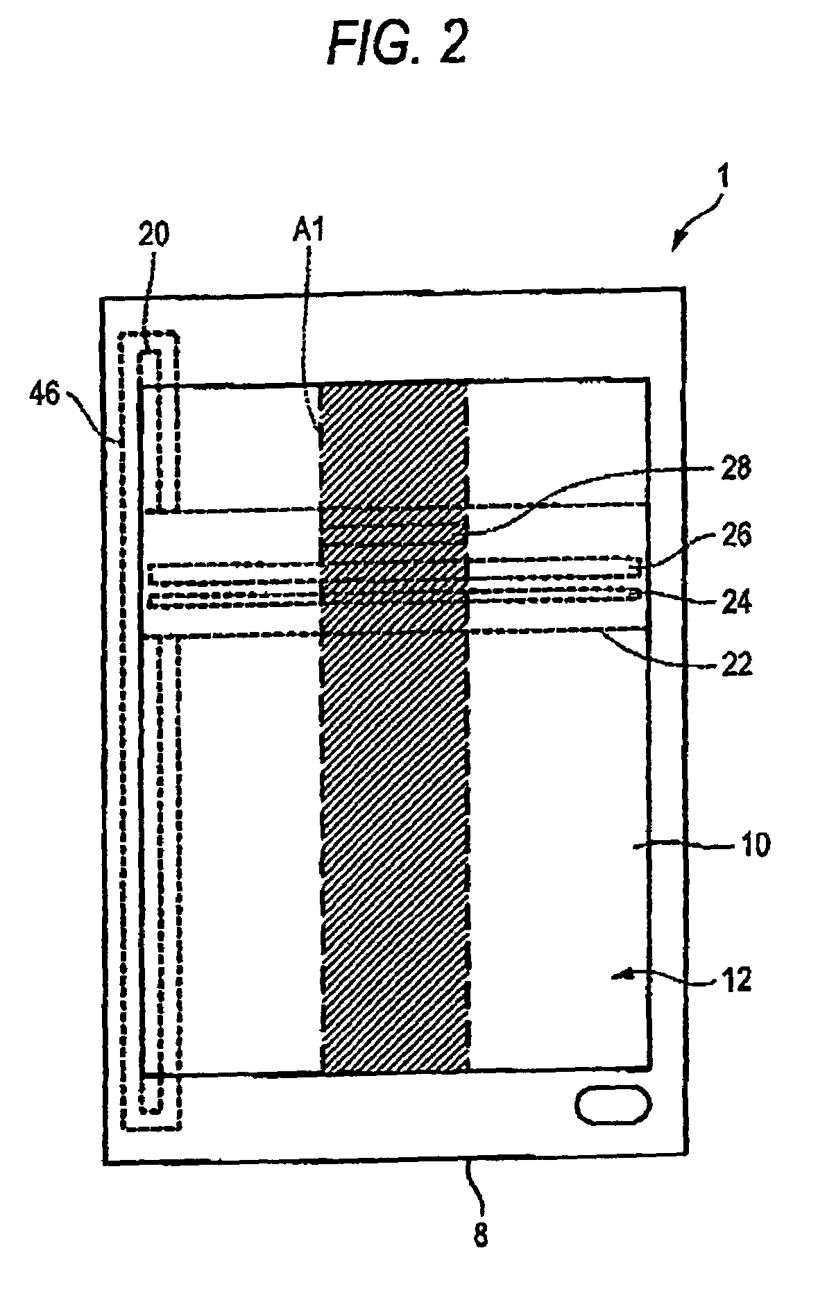
[0051]FIG. 2 to FIG. 4 are schematic diagrams showing an image scanner 1, which is an image reading device of a first embodiment of the present invention. Image scanner 1 is a so-called flatbed image scanner. Image scanner 1 can read reflection originals 4 (see FIG. 4A) and transmission originals of up to A4 size and A4 letter size. A reflection original 4, which is a first object, is a printed document or photograph, etc. A transmission original, which is a second object, is a 35 mm film (negative or positive film) 6 (see FIG. 4B), etc. In the description, that follows, 35 mm film 6 shall be used as the transmission original. The image reading device may be a sheet-feed type image scanner or a copier. The transmission original is not restricted to 35 mm film 6.

[0052]A housing 8 is formed to have a box shape with an open upper side and supports an original platen 10 on its open side. Original platen 10 is formed substantially of a rectangular glass plate or other transparent plate. ...

second embodiment

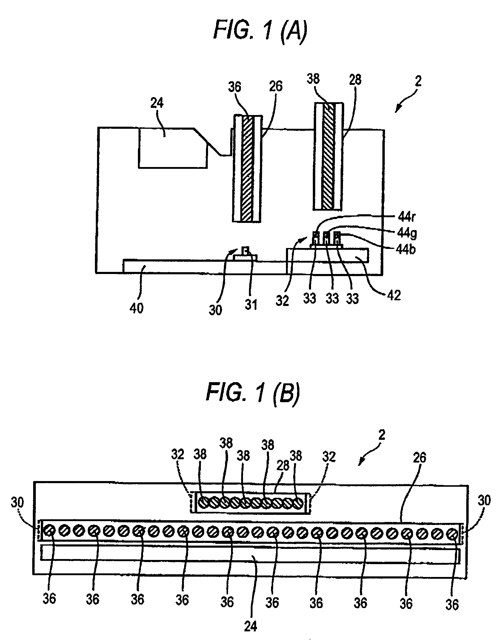
[0094]With a contact image sensor module 2 according to the second embodiment of the present invention, a first image sensor 30 and a second image sensor 32 are mounted on the same printed circuit board 40 (see FIG. 10). For the second embodiment, parts that are practically the same as those of the first embodiment shall be provided with the same symbols and description thereof shall be omitted.

[0095]The focal length of a first rod lens array 26 differs from the focal length of a second rod lens array 28. First image sensor 30 and second image sensor 32 are mounted on the same printed circuit board 40. The focal length of first rod lens array 26 is designed so that the focal point position due to first image sensor 30 and first rod lens array 26 will be at platen surface 12 of original platen 10. The focal length of second rod lens array 28 is designed so that the focal point position due to second image sensor 32 and second rod lens array 28 will be at a position 1 mm away from pla...


PUM


Abstract

A contact image sensor module includes: a first image sensor, having a first light receiving element set aligned in a straight line; a second image sensor, having a second light receiving element set aligned in parallel to the abovementioned first light receiving element set; a first lens unit, forming, on the abovementioned first light receiving element set, a clear image of a first object, which is positioned at a first distance from light receiving surfaces of the abovementioned first light receiving element set; and a second lens unit, forming, on the abovementioned second light receiving element set, a clear image of a second object, which is positioned at a second distance, differing from the above mentioned first distance, from the light receiving surfaces of the abovementioned first light receiving element set.

Description

BACKGROUND OF THE INVENTION[0001]The present invention relates to a contact image sensor module and an image reading device equipped with the same.[0002]Image reading devices equipped with a contact image sensor module (see Patent Document 1) have been generally known. Since a contact image sensor module is short in the optical path of the optical system, an image reading device can be made compact readily.[0003]However, since a contact image sensor module is shallow in the depth of field, an original that is positioned at a position away from a platen surface of an original platen cannot be read clearly. For example, the image reading device described in Patent Document 1 cannot read a 35 mm film, held in a holder, etc., clearly.[0004]The image reading devices described in Patent Documents 2 and 3 are equipped with a plurality of optical systems and can clearly read reflection originals and transmission originals by the switching of the optical path in accordance with the original....

Claims


Application Information

Patent Timeline
Patent Type & Authority Patents(United States)
IPC IPC(8): H04N1/04H04N1/46
CPCH04N1/0402H04N1/0408H04N1/0423H04N1/0449H04N1/0464H04N1/0467
Inventor OHARA, TOSHIMITSUNAKANO, KAZUHIRO
Owner SEIKO EPSON CORP
Why Eureka
Try Eureka