Method for manufacturing array substrate of translucent LCD

a technology of translucent lcd and array substrate, which is applied in the direction of optics, instruments, electrical equipment, etc., can solve the problems of high power consumption of backlight, inability to use reflective lcds, and easy light emission, so as to improve both the reflectivity properties in the reflective region, and improve the contact resistance in the transmissive region. , the effect of improving the reflectivity

Active Publication Date: 2009-01-20
HYDIS TECH CO LTD
View PDF7 Cites 22 Cited by
  • Summary
  • Abstract
  • Description
  • Claims
  • Application Information

AI Technical Summary

Benefits of technology

[0022]Accordingly, the present invention has been made to solve the above-mentioned problems occurring in the prior art, and an object of the present invention is to provide a method for manufacturing an array substrate of a translucent LCD capable of simultaneously forming source and drain metal layers as reflective electrodes while improving both the contact resistance in a transmissive region and the reflectivity properties in a reflective region.
[0023]Another object of the present invention is to provide a method for manufacturing an array substrate of a translucent LCD capable of improving both the contact resistance in a transmissive region and the reflectivity properties in a reflective region for stable operation while securing excellent screen quality.
[0024]Still another object of the present invention is to provide a method for manufacturing an array substrate of a translucent LCD capable of reducing the number of mask processes for process simplification and manufacturing cost saving.

Problems solved by technology

However, much power is consumed by the backlight.
However, reflective LCDs cannot be used when the surroundings are dark.
However, any metal belonging to Al series has high contact resistance with ITO, which constitutes the pixel electrodes, and does not emit light easily.
Even when light is emitted, mura and luminance deteriorate.
This degrades screen quality.
However, Ag-series metal is expensive and is practically impossible to use, considering the production cost.
In summary, conventional translucent LCDs using source and drain metal layers as reflective electrodes cannot meet consumers' expectations, due to problems related to contact resistance with the ITO layer and increased cost.
Consequently, conventional methods for manufacturing an array substrate of a translucent LCD, which require at least 8 masks, are very complicated and incur great costs.

Method used


Image

  • Method for manufacturing array substrate of translucent LCD
  • Method for manufacturing array substrate of translucent LCD
  • Method for manufacturing array substrate of translucent LCD

Examples


Embodiment Construction

[0046]Hereinafter, a preferred embodiment of the present invention will be described with reference to the accompanying drawings. In the following description and drawings, the same reference numerals are used to designate the same or similar components, and so repetition of the description on the same or similar components will be omitted.

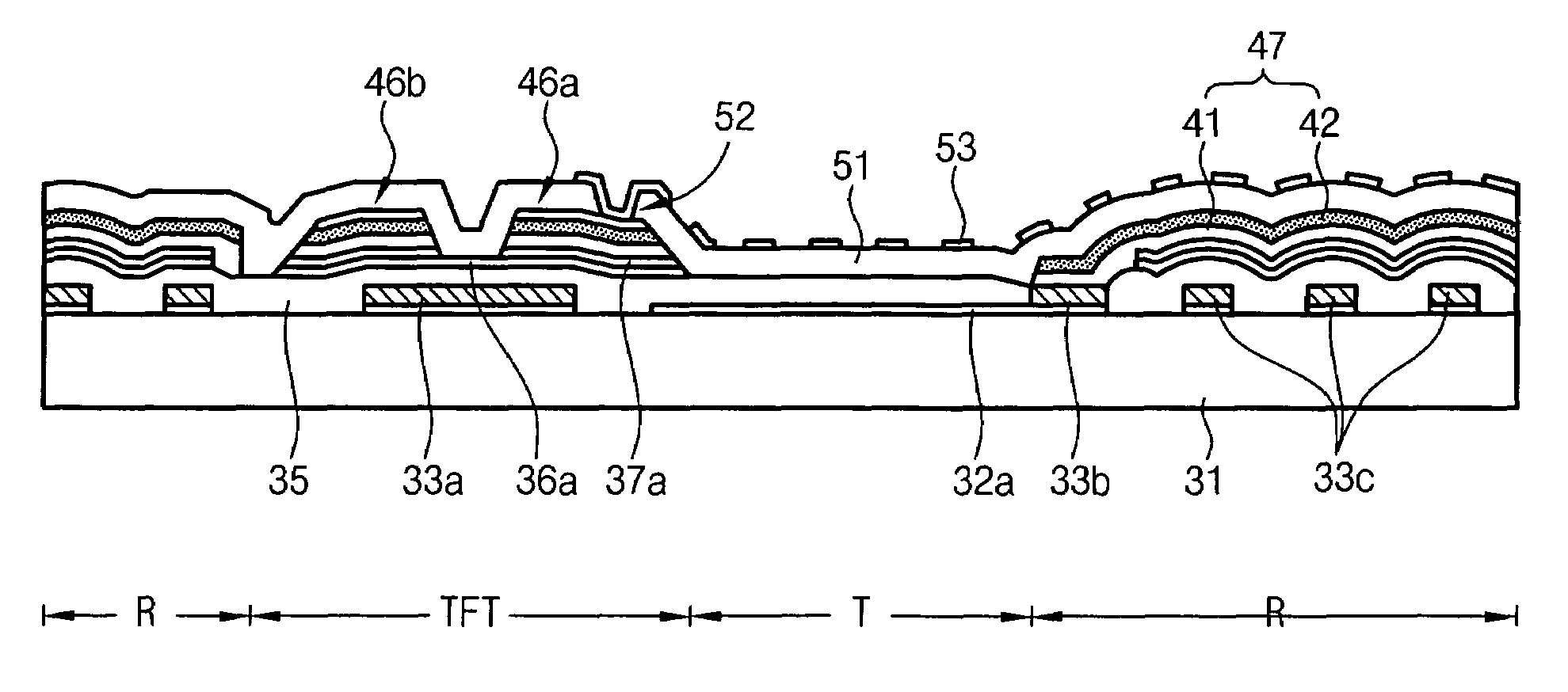
[0047]The present invention uses a triple layer of Mo—Al—Mo to form source and drain electrodes, as well as a reflective electrode. In a reflective region, the top Mo is removed to expose the Al metal layer, which has a high reflectivity and, in a TFT region, the top Mo remains intact. This secures an excellent level of reflectivity in the reflective region and good electrical contact in the TFT region. As a result, the screen quality of products improves, and the production cost can be reduced by using inexpensive Mo and Al.

[0048]In addition, the present invention utilizes half-tone exposure technology to manufacture an array substrate of a trans...


PUM

PropertyMeasurementUnit
translucentaaaaaaaaaa
thicknessaaaaaaaaaa
photosensitiveaaaaaaaaaa

Abstract

Disclosed is a method for manufacturing an array substrate of a translucent LCD capable of simultaneously forming source and drain metal layers as reflective electrodes while improving both the contact resistance in a transmissive region and the reflectivity properties in a reflective region. The source and drain metal layers have a triple-layered structure of Mo—Al—Mo and, the top Mo is selectively removed from the reflective region. As a result, the screen quality of products improves. In addition, about 5-6 masks are enough to manufacture an array substrate using half-tone exposure technology, in contrast to the prior art which uses 8-11 masks. As the number of masks and processes is reduced in this manner, the manufacturing cost decreases accordingly and the process is simplified.

Description

BACKGROUND OF THE INVENTION[0001]1. Field of the invention[0002]The present invention relates to a method for manufacturing a translucent LCD, and more particularly to a method for manufacturing an array substrate of a translucent LCD capable of providing low contact resistance in a transmissive region and high reflectivity properties in a reflective region while simplifying processes.[0003]2. Description of the Prior Art[0004]As generally known in the art, LCDs include two substrates having electrodes formed thereon and a liquid crystal layer interposed between them. By applying a voltage to the electrodes, liquid crystal molecules in the liquid crystal layer are rearranged. As a result, the amount of transmitted light is adjusted, and predetermined images are realized.[0005]LCDs may be classified into transmissive LCDs using a light source, such as a backlight, to display images and reflective LCDs using natural light as the light source. The transmissive LCDs can realize bright i...

Claims


Application Information

Patent Timeline
Patent Type & Authority Patents(United States)
IPC IPC(8): G02F1/136
CPCG02F1/133555G02F1/134309G02F2001/136231G02F1/136231G02F1/136
Inventor KIM, BYUNG HOONIHM, SAM HO
Owner HYDIS TECH CO LTD
Why Eureka
Try Eureka