Testing method detecting localized failure on a semiconductor wafer

a technology of localized failure and test method, which is applied in the direction of semiconductor/solid-state device testing/measurement, instruments, measurement devices, etc., can solve the problems of increasing the yield of ever more complicated semiconductor chips, unacceptably low, and increasing the respective margins associated with constituent fabrication processes. achieve the effect of intelligent approach and greater real-time access to defectives

Active Publication Date: 2009-04-07
SAMSUNG ELECTRONICS CO LTD
View PDF21 Cites 7 Cited by
  • Summary
  • Abstract
  • Description
  • Claims
  • Application Information

AI Technical Summary

Benefits of technology

[0014]Embodiments of the invention provide a more intelligent approach to the identification and separation of defective wafers from acceptable wafers within a fabrication lot. The failure analysis thresholding used by embodiments of the invention is no longer limited to only a simple pass / fail target yield. Rather, embodiments of the invention are able identify and account for localized failures on a wafer. Additionally, embodiments of the invention are adapted to provide information to on a wafer by wafer basis, rather than on a lot by lot basis, thereby enabling greater real-time access to defective and / or acceptable wafers within a lot.

Problems solved by technology

Increasing the yield of ever more complicated semiconductor chips is not easy.
Contemporary semiconductor chips are fabricated on a wafer using a very complex sequence of different processes.
Indeed, as integration densities for contemporary semiconductor chips have increased over the past several decades, the respective margins associated with constituent fabrication processes have become increasingly restrictive.
Where an individual wafer within a lot is determined to be defective (e.g., it exhibits an unacceptably low yield), it may be removed from the fabrication process and subjected to a detailed failure analysis.
This detailed failure analysis is an expensive and time-consuming process, but it is also a principal step towards improving yield.
Those wafers exhibiting an actual yield below the target yield are deemed defective and sent to failure analysis.
Such a simplistic approach to separating defective and acceptable wafers has proved increasingly unsatisfactory.
Further, conventional wafer level testing practices do not provide information on any basis other than a lot by lot basis.
Again, this information granularity level is also proving to be increasingly unsatisfactory.

Method used


Image

  • Testing method detecting localized failure on a semiconductor wafer
  • Testing method detecting localized failure on a semiconductor wafer
  • Testing method detecting localized failure on a semiconductor wafer

Examples


Embodiment Construction

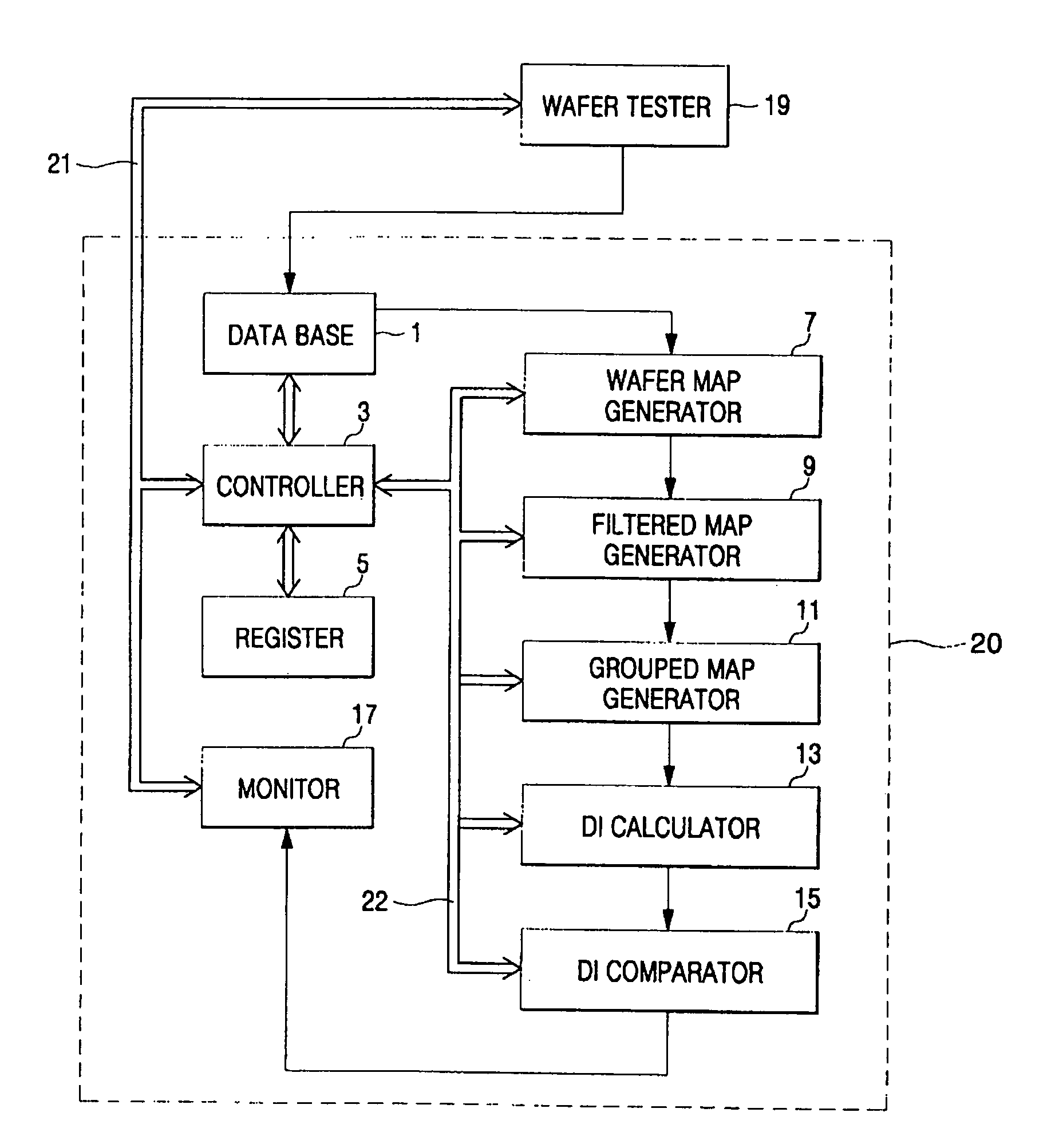
[0031]Selected features and advantages associated with several embodiments of the invention are described hereafter with reference to the accompanying drawings. The invention may, however, be implemented in various embodiments. The nature, construction, and compostion of elements and / or steps in the following embodiments may be modified without removing such modifications from the actual scope of the invention as defined by the attached claims.

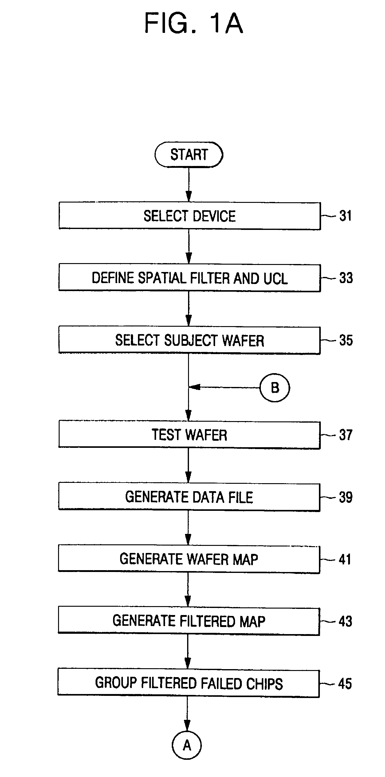
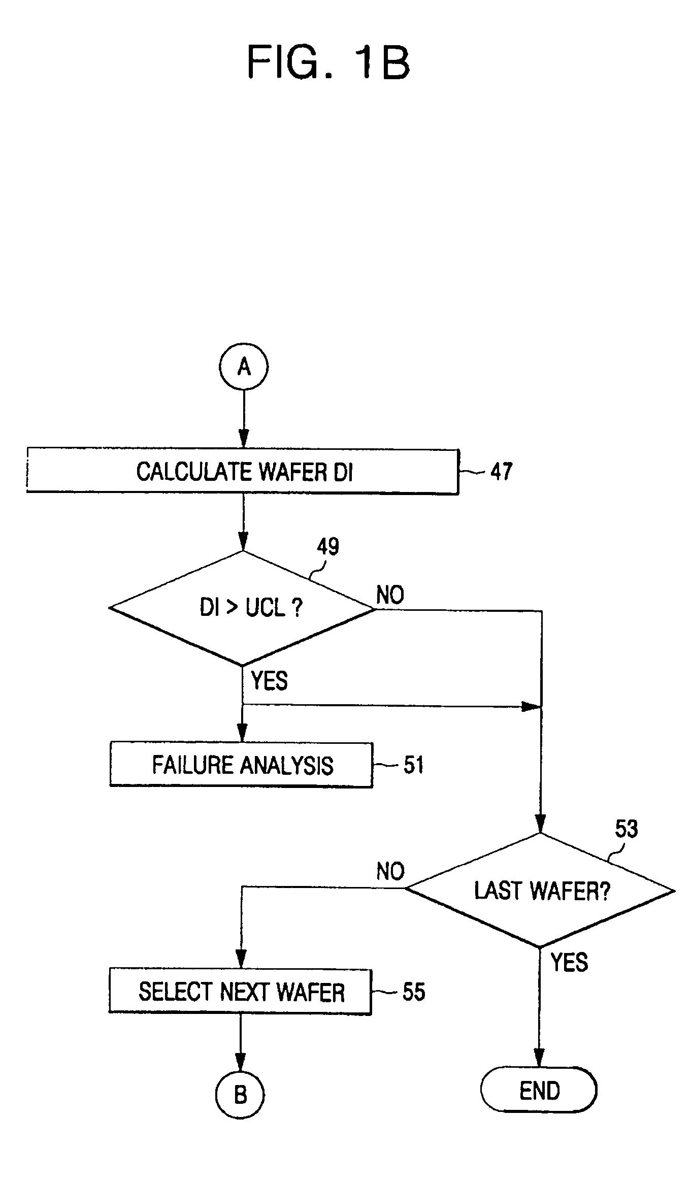
[0032]In particular, an exemplary test method according to one embodiment of the invention is described hereafter in relation to the flowchart shown in FIGS. 1A and 1B. In the description of this embodiment, certain functions and method interrelationships are referred to as “steps”. This step by step approach to explaining the use of an exemplary test method should not be given an overly-literal interpretation. The steps are merely explanatory references. In actual implementation, the exemplary steps might be combined or further partitioned, r...


PUM


Abstract

A method and system for testing a wafer comprising semiconductor chips are disclosed. A determination of whether or not the wafer is defective is made in relation to a spatially related group of filtered failed semiconductor chips on the wafer, where the spatially related group corresponds to a localized failure on the wafer and is used to calculate a defect index value.

Description

BACKGROUND OF THE INVENTION[0001]1. Field of the Invention[0002]Embodiments of the invention relate generally to a method and system for testing semiconductor chips on a wafer. More particularly, embodiments of the invention relate to a test method and system identifying a localized failure of semiconductor chips on a wafer.[0003]2. Description of the Related Art[0004]The functional heart of all semiconductor devices is an integrated circuit formed on a die of semiconductor compatible material. This die is commonly referred to as a semiconductor “chip.” Semiconductor chips are commercially fabricated in great numbers on material wafers. Wafers are most typically formed from a polished slice of silicon material, but other materials may be used.[0005]The business of fabricating semiconductor chips is a highly competitive one, and fabrication yield (i.e., the percentage of semiconductor chips that actually work out of a total batch of semiconductor chips fabricated on a wafer) is an im...

Claims


Application Information

Patent Timeline
Patent Type & Authority Patents(United States)
IPC IPC(8): G01R31/26
CPCG01R31/31718G01R31/318511H01L22/00
Inventor KANG, JOONG-WUKCHEONG, KWANG-YUNG
Owner SAMSUNG ELECTRONICS CO LTD
Why Eureka
Try Eureka