Electrical measurements on semiconductors using corona and microwave techniques

Inactive Publication Date: 2009-04-21
KLA TENCOR CORP
View PDF4 Cites 15 Cited by
  • Summary
  • Abstract
  • Description
  • Claims
  • Application Information

AI Technical Summary

Benefits of technology

[0014]A corona-microwave system can generate accurate capacitance-voltage (C-V) and resistance-voltage (R-V) curves, thereby allowing the accurate determination of gate film capacitance, sheet resistance of implanted regions, and mobility of a substrate under a gate. The corona-microwave system can advantageously combine a corona deposition system, a Kelvin probe, and a microwave probe.
[0015]Using this corona-microwave system, the corona deposition system can deposit a corona charge on a surface of the semiconductor. The Kelvin probe can be used to make a first electrical measurement of a layer of the semiconductor, whereas the microwave probe can be used to make a second electrical measurement of that layer. The steps of charge deposition and probe measurements can be repeated to generate a curve plotting the first and second electrical measurements. Because the first and second electrical measurements can be accurately made, the extracted information from the curve is also accurate.
[0016]In one embodiment for determining gate dielectric parameters, the corona charge is deposited on a test gate electrode, wherein the Kelvin probe can measure a voltage (i.e. the first electrical measurement) of a gate film formed under the test gate electrode and the microwave probe can measure a capacitance (i.e. the second electrical measurement). In this case, the microwave probe is operated in its capacitive measurement mode by measuring a shift in resonant frequency of its microwave cavity as the microwave probe is pulled up from the gate film. Thus, in this embodiment, the corona-micr

Problems solved by technology

Unfortunately, each of these techniques has entailed significant disadvantages.
Unfortunately, because of the small area associated with charge deposition, it is difficult to get an accurate measure of the amount of charge deposited during step 101, thereby preventing an accurate measurement of the capacitance in step 104.
Technique 200, albeit accurate, has the disadvantage requiring actual construction of the complete transistor and its connected pad before the measurement can be made.
Unfortunately, microwave probe 310 is sensitive to both the sheet resistance of the shallow implanted region as well as the sheet resistance of the substrate bel

Method used


Image

  • Electrical measurements on semiconductors using corona and microwave techniques
  • Electrical measurements on semiconductors using corona and microwave techniques
  • Electrical measurements on semiconductors using corona and microwave techniques

Examples


Example

DETAILED DESCRIPTION OF THE FIGURES

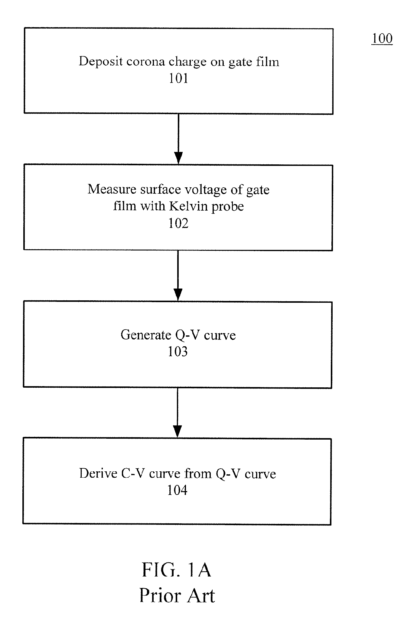
[0034]A corona-microwave probe system can make accurate electrical measurements. Using these accurate electrical measurements, the corona-microwave system can generate accurate information regarding gate dielectric parameters, the mobility of a substrate, and the sheet resistance of implant regions. As described in further detail below, the corona-microwave probe system can advantageously make capacitance measurements directly, rather than by derivation, thereby improving accuracy. Moreover, the corona-microwave probe system can advantageously eliminate the need to construct a physical transistor connected to a pad to measure substrate mobility as well as the need to physically contact the wafer to measure sheet resistance.

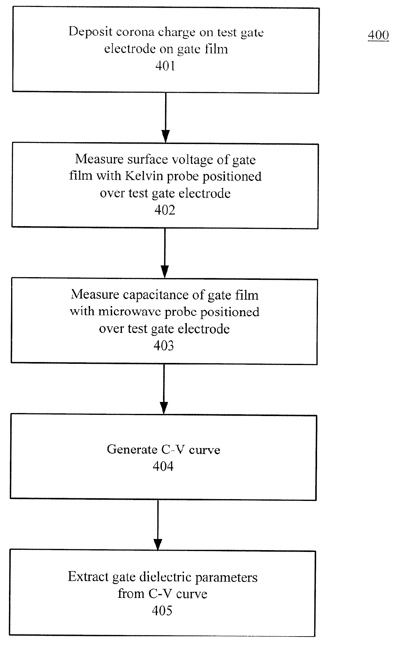
[0035]FIG. 4A illustrates a technique 400 for generating an accurate C-V curve. In technique 400, step 401 can deposit corona charge on a test gate electrode structure formed on a gate film. In step 402, a Kelvin probe, which is ...


PUM


Abstract

A corona-microwave system can generate accurate capacitance-voltage (C-V) and resistance-voltage (R-V) curves, thereby allowing the accurate determination of gate film capacitance, sheet resistance of implanted regions, and mobility of a substrate under a gate. The corona-microwave system can combine a corona deposition system, a Kelvin probe, and a microwave probe. The corona deposition system can deposit a corona charge on a surface of the semiconductor. The Kelvin and microwave probes can be used to make first and second electrical measurements of a layer/region of the semiconductor. The steps of charge deposition and probe measurements can be repeated to generate a curve plotting the first and second electrical measurements. Because the first and second electrical measurements can be accurately made, the extracted information from the curve is also accurate.

Description

RELATED APPLICATIONS[0001]This application claims priority of U.S. Provisional Patent Application 60 / 669,196, entitled “New Technique For Electrical Measurements On Semiconductors” filed Apr. 6, 2005.BACKGROUND OF THE INVENTION[0002]1. Field of the Invention[0003]The invention relates to the field of semiconductor metrology, and in particular, to an improved system and method for performing various electrical measurements using combined corona and microwave techniques.[0004]2. Related Art[0005]Various electrical measurements can be done on a semiconductor wafer to determine the performance characteristics of the devices formed on that semiconductor wafer. Exemplary electrical measurements include capacitance, sheet resistance (i.e. the resistance of very thin doped regions in a substrate), and mobility (i.e. the relationship between resistivity and charge density (resistivity / charge density) associated with the surface of stressed (using compression or tensile forces) silicon). Each...

Claims


Application Information

Patent Timeline
IPC IPC(8): G01R31/302
CPCG01R31/2621G01R31/311
Inventor JANIK, GARY R.
Owner KLA TENCOR CORP
Why Eureka
Try Eureka