Semiconductor memory device including floating body memory cells and method of operating the same

a memory device and semiconductor technology, applied in the field can solve the problems of complicated circuit configuration, limit in reducing the physical layout area of semiconductor memory devices,

Active Publication Date: 2009-11-17
SAMSUNG ELECTRONICS CO LTD
View PDF10 Cites 2 Cited by
  • Summary
  • Abstract
  • Description
  • Claims
  • Application Information

AI Technical Summary

Problems solved by technology

However, because the conventional dynamic memory cell depends on the capacitor, when a memory cell array includes such dynamic memory cells, there is a limit in reducing the physical layout area of the semiconductor memory device.
The transistor stores many carriers in the floating body, and needs to be refreshed because the stored carriers are lost in a predetermined amount of time.
Also, the conventional semiconductor memory device shown in FIG. 1 requires a complicated circuit configuration for the data read operation.

Method used


Image

  • Semiconductor memory device including floating body memory cells and method of operating the same
  • Semiconductor memory device including floating body memory cells and method of operating the same
  • Semiconductor memory device including floating body memory cells and method of operating the same

Examples


Embodiment Construction

[0047]The present invention will now be described more fully with reference to the accompanying drawings, in which exemplary embodiments of the invention are shown. The invention, however, may be embodied in various different forms, and should not be construed as being limited only to the illustrated embodiments. Rather, these embodiments are provided as examples, to convey the concept of the invention to one skilled in the art. Accordingly, known processes, elements, and techniques are not described with respect to some of the embodiments of the present invention. Throughout the drawings and written description, like reference numerals will be used to refer to like or similar elements.

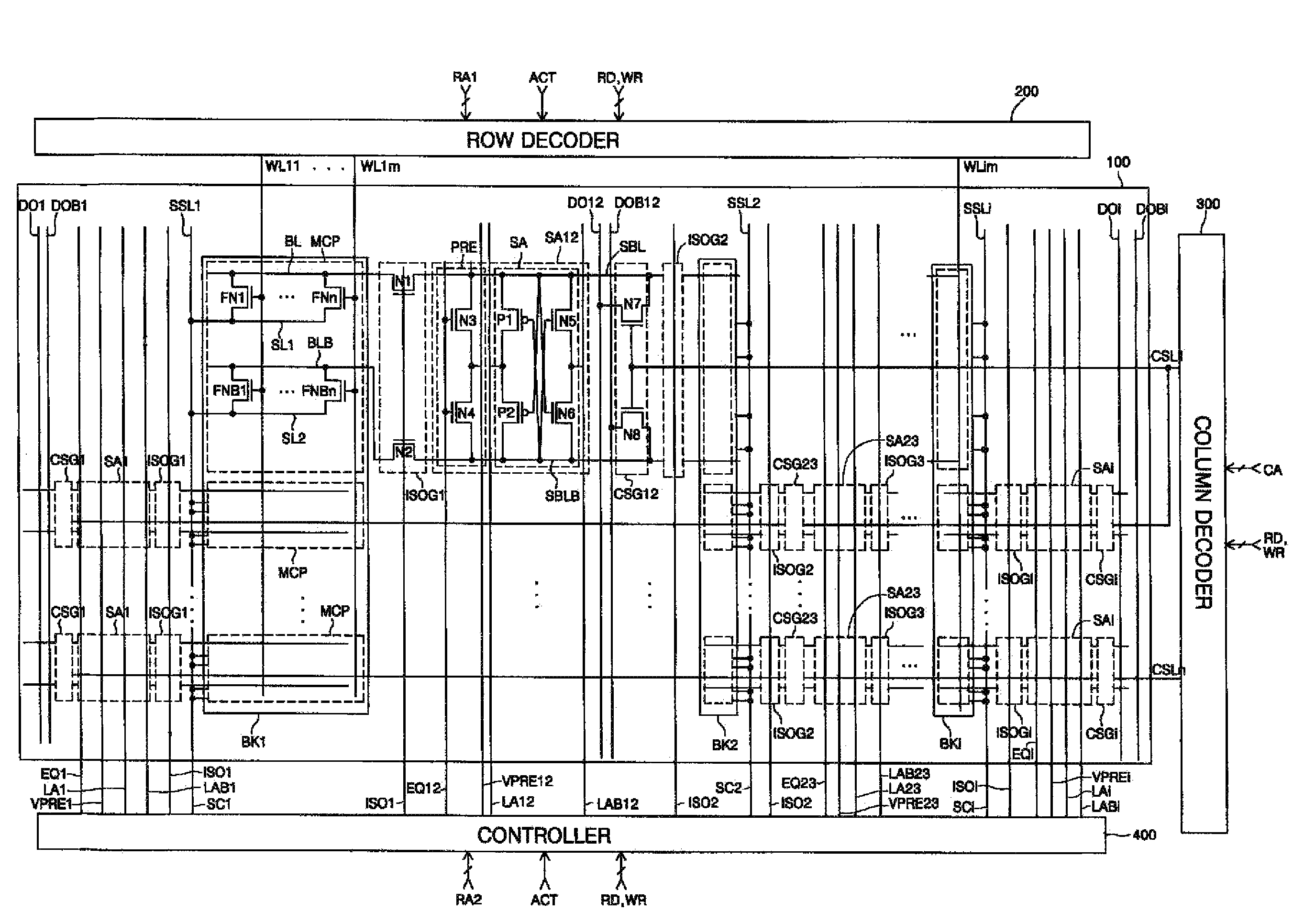
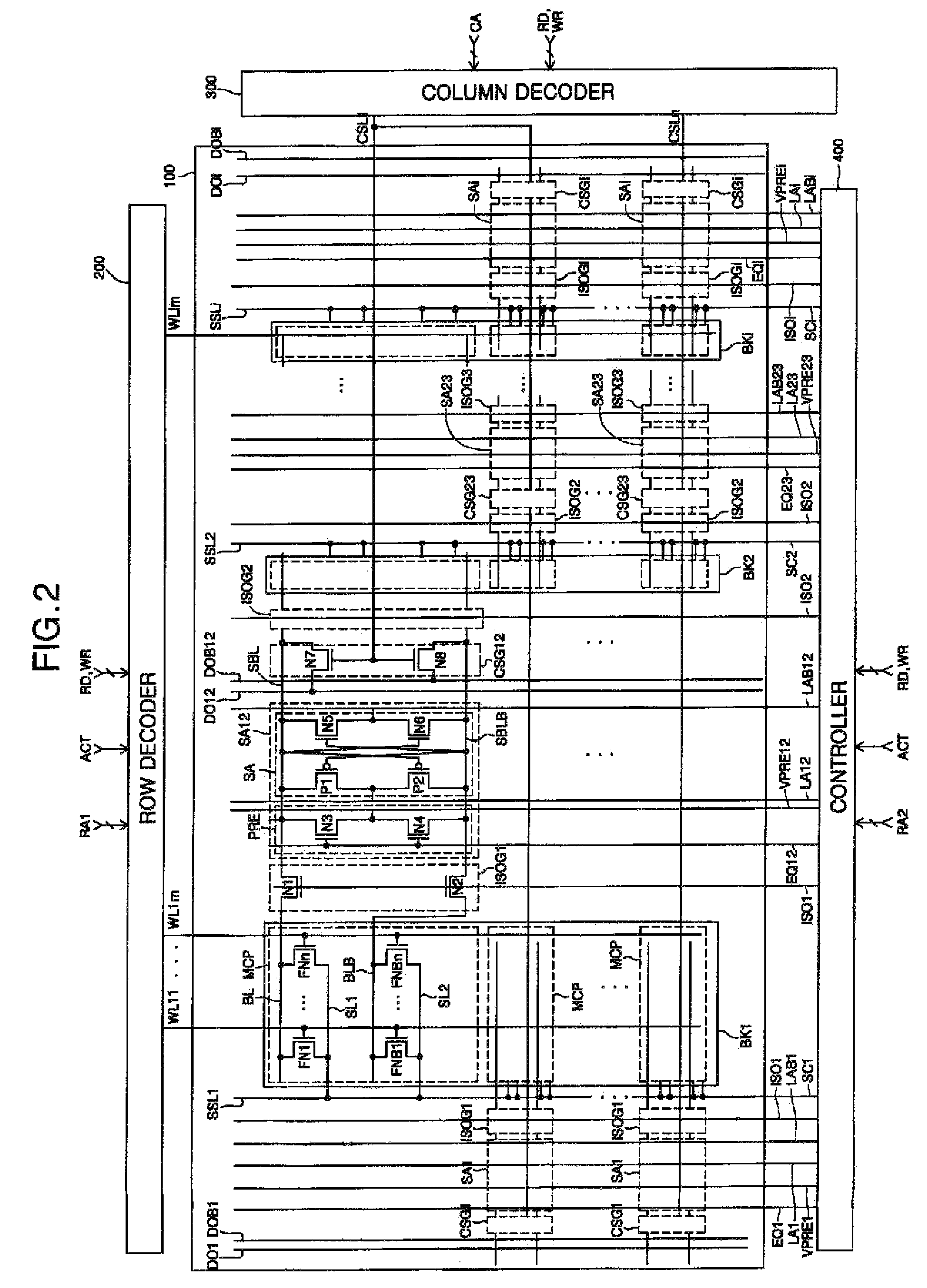
[0048]FIG. 2 is a block diagram showing the construction of a semiconductor memory device, according to an illustrative embodiment of the present invention.

[0049]Referring to FIG. 2, the semiconductor memory device includes a memory cell array 100, a row decoder 200, a column decoder 300 and a control...


PUM


Abstract

A semiconductor memory device includes first and second memory cells having floating bodies, each of which includes a gate connected to a word line and an electrode connected to a common source line to store data. A controller applies a first voltage to the common source line, a negative second voltage to the word line, a third voltage as a first sense enable control voltage and the first voltage as a second sense enable control voltage during a first write period of a write operation. The controller also applies a fourth voltage to the common source line and the first voltage to the word line during a second write period of the write operation. The sensing portion amplifies a bit line and an inverted bit line to the third voltage or the first voltage, respectively, during the first write period in response to the first and second sense enable control voltages.

Description

[0001]A claim of priority is made to Korean Patent Application No. 2006-0117028, filed Nov. 24, 2006, the subject matter of which is hereby incorporated by reference.BACKGROUND OF THE INVENTION[0002]1. Field of the Invention[0003]The present invention relates to a semiconductor memory device, and more particularly, the present invention relates to a semiconductor memory device having floating body memory cells and a method of operating the same.[0004]2. Description of Related Art[0005]In general, a dynamic random access memory (DRAM) device, which is one type of semiconductor memory device, includes a dynamic memory cell that includes a transistor and a capacitor, such that data “0” or “1” is determined depending on whether or not the capacitor is charged with electric charges. Since electric charges charged in the capacitor are lost in a predetermined amount of time, a refresh operation is necessary.[0006]However, because the conventional dynamic memory cell depends on the capacito...

Claims


Application Information

Patent Timeline
Patent Type & Authority Patents(United States)
IPC IPC(8): G11C16/04
CPCG11C11/404G11C11/4076G11C2211/4016G11C11/4074G11C11/4091G11C11/4094
Inventor PARK, DUK-HASONG, KI-WHANKIM, JIN-YOUNG
Owner SAMSUNG ELECTRONICS CO LTD
Why Eureka
Try Eureka