

Semiconductor package having leadframe with exposed anchor pads
a technology of anchor pads and semiconductors, applied in semiconductor devices, semiconductor/solid-state device details, electrical apparatus, etc., can solve the problems of increasing the risk of shorting, difficult circuit routing of the underlying printed circuit board underneath the exposed die pad, and increasing the need of space availability, so as to achieve high-density circuit routing
- Summary
- Abstract
- Description
- Claims
- Application Information
AI Technical Summary
Problems solved by technology
Method used
Image

Examples
first embodiment
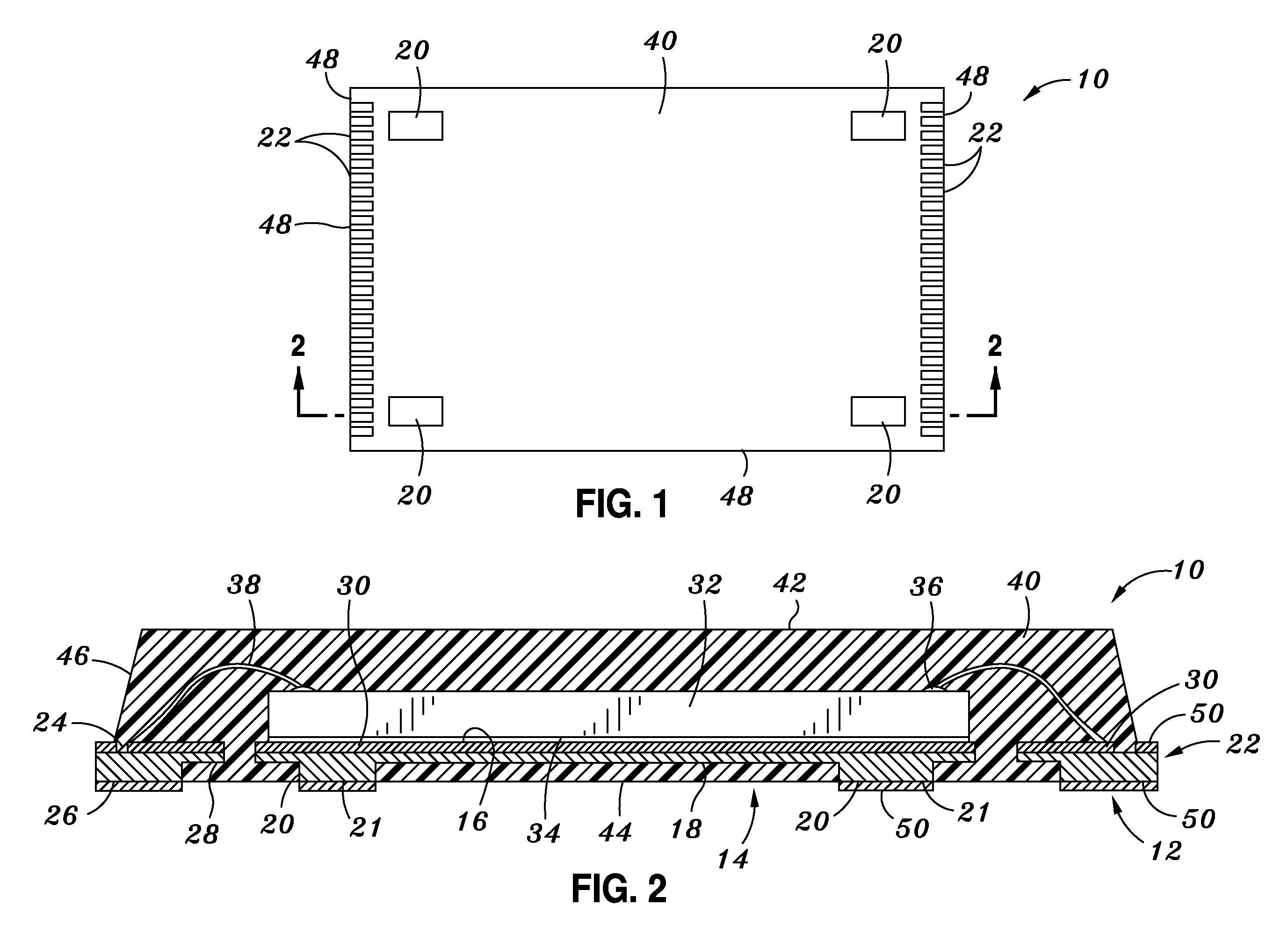
[0022]Referring now to the drawings wherein the showings are for purposes of illustrating various embodiments of the present invention only, and not for purposes of limiting the same, FIGS. 1 and 2 depict a semiconductor package 10 constructed in accordance with the present invention. The semiconductor package 10 comprises a leadframe 12 which itself includes a die attach pad or die pad 14. In the semiconductor package 10, the die pad 14 has a generally quadrangular configuration defining four (4) peripheral edge segments. In addition, the die pad 14 defines a generally planar top surface 16, and an opposed, generally planar bottom surface 18.
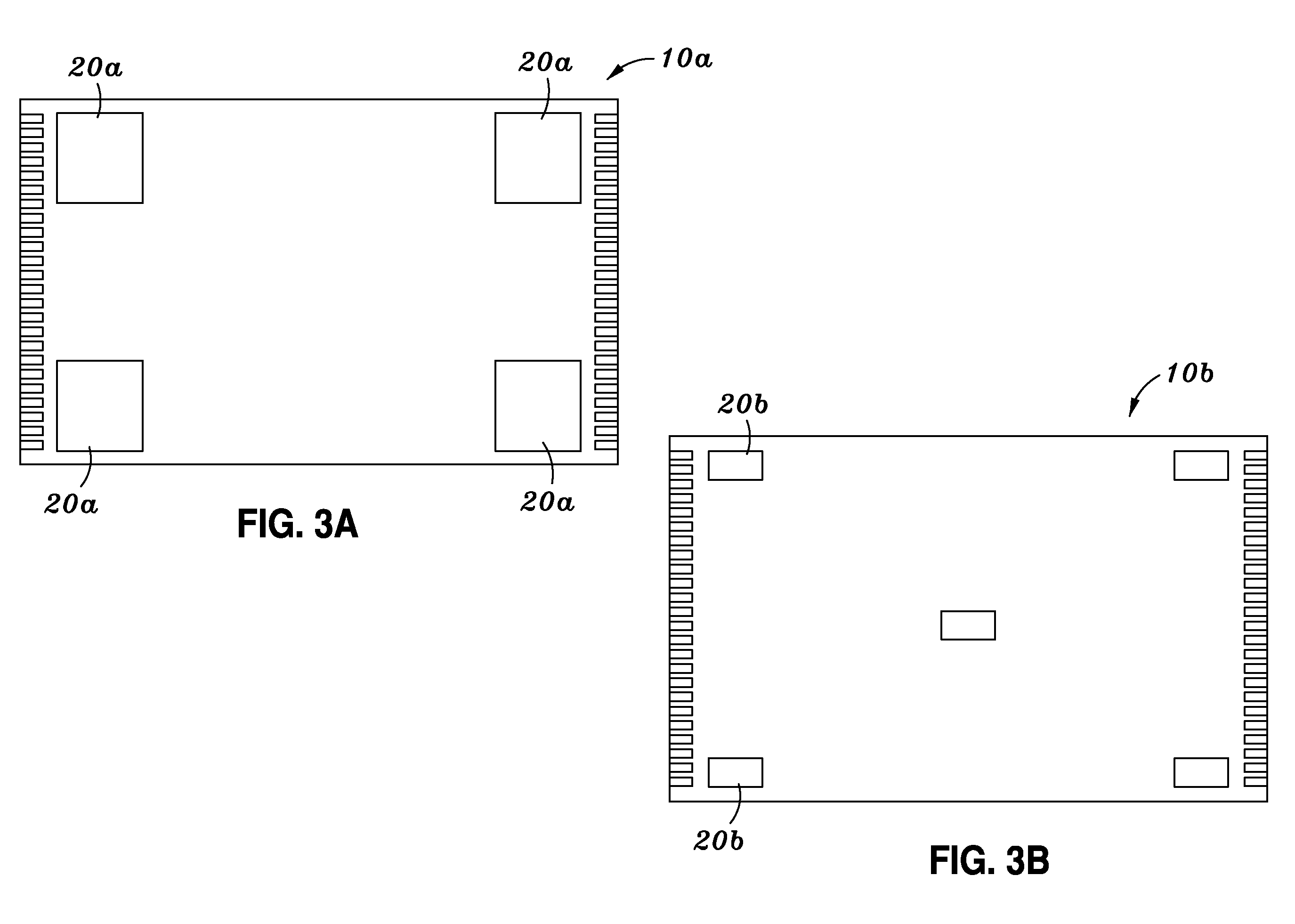
[0023]The die pad 14 of the leadframe 12 further includes a plurality of anchor pads 20 which protrude downwardly from the bottom surface 18 in the manner shown in FIG. 2. As seen in FIG. 1, the die pad 14 of the semiconductor package 10 is provided with four (4) identically configured anchor pads 20, each of which has a generally quadrangular ...
second embodiment
[0036]Referring now to FIG. 4, there is shown a semiconductor package 100 constructed in accordance with the present invention. The semiconductor package 100 comprises a leadframe 112 which includes a die attach pad or die pad 114. In the semiconductor package 100, the die pad 114 has a generally quadrangular configuration defining four (4) peripheral edge segments. In addition, the die pad 114 defines a generally planar top surface 116, and an opposed, generally planar bottom surface 118. In addition to the top and bottom surfaces 116, 118, the die pad 114 further defines a shoulder or shelf 119 which is recessed relative to the bottom surface 118, and extends in opposed relation to the top surface 116. The shelf 119 also preferably circumvents the bottom surface 118.
[0037]In addition to the die pad 114, the leadframe 112 of the semiconductor package 100 comprises a plurality of leads 122. As in the semiconductor package 10 described above, the leads 122 of the semiconductor packag...
third embodiment
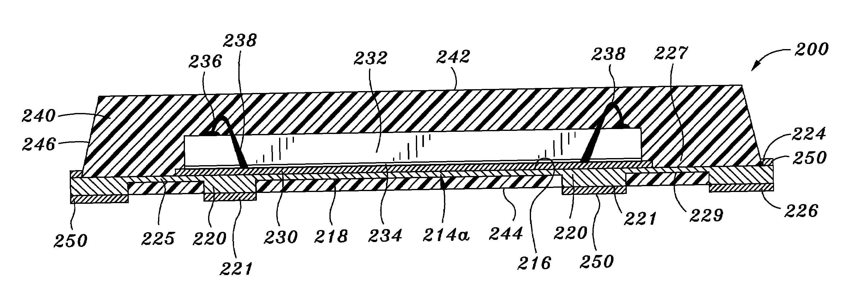
[0046]Referring now to FIGS. 5 and 6, there is shown a semiconductor package 200 constructed in accordance with the present invention. The semiconductor package 200 comprises a leadframe 212 which itself includes a plurality of separate die attach pad sections or die pad sections 214a, 214b, 214c which are disposed in spaced relation to each other. Each of the die pad sections 214a, 214b, 214c defines a generally planar top surface 216, and an opposed, generally planar bottom surface 218. Each of the die pad sections 214a, 214b, 214c of the leadframe 212 further includes at least one anchor pad 220 which protrudes downwardly from the bottom surface 218 thereof in the manner shown in FIG. 6. As seen in FIG. 5, the die pad section 214a of the semiconductor package 200 is provided with two (2) identically configured anchor pads 220, each of which has a generally quadrangular configuration. The die pad sections 214b, 214c are each provided with one (1) anchor pad 220 which also has a ge...
PUM
 Abstract
Description
Claims
Application Information