Semiconductor device with increased I/O leadframe

a semiconductor and leadframe technology, applied in semiconductor devices, semiconductor/solid-state device details, electrical apparatus, etc., can solve the problems of increasing the overall size of the qfp package, further limiting the number of inputs/outputs (i/o's) which may be included therein, and conventional leadframe structures as currently known and integrated into existing qfp packages often prove unsatisfactory, so as to achieve the effect of effectively electrically isolating various leads from each

Active Publication Date: 2011-08-30
AMKOR TECH SINGAPORE HLDG PTE LTD
View PDF436 Cites 27 Cited by
  • Summary
  • Abstract
  • Description
  • Claims
  • Application Information

AI Technical Summary

Benefits of technology

[0013]In accordance with the present invention, there is provided a semiconductor package (e.g., a QFP package) including a uniquely configured leadframe sized and configured to maximize the available number of exposed leads in the semiconductor package. More particularly, the semiconductor package of the present invention includes a generally planar die pad or die paddle defining multiple peripheral edge segments. In addition, the semiconductor package includes a plurality of leads. Some of these leads include exposed bottom surface portions or lands which are provided in at least one row or ring which at least partially circumvents the die pad, with other leads including portions which protrude from respective side surfaces of a package body of the semiconductor package. Connected to the top surface of the die pad is at least one semicond...

Problems solved by technology

One of the deficiencies of currently known QFP packages is attributable to the length at which the leads protrude from the sides of the package body, such protrusion length resulting in an increase in the overall size of the QFP package and further limiting the number of inputs/outputs (I/O's) which may be included therein.
In view of this need, conventional leadframe structures as currently known ...

Method used


Image

  • Semiconductor device with increased I/O leadframe
  • Semiconductor device with increased I/O leadframe
  • Semiconductor device with increased I/O leadframe

Examples


first embodiment

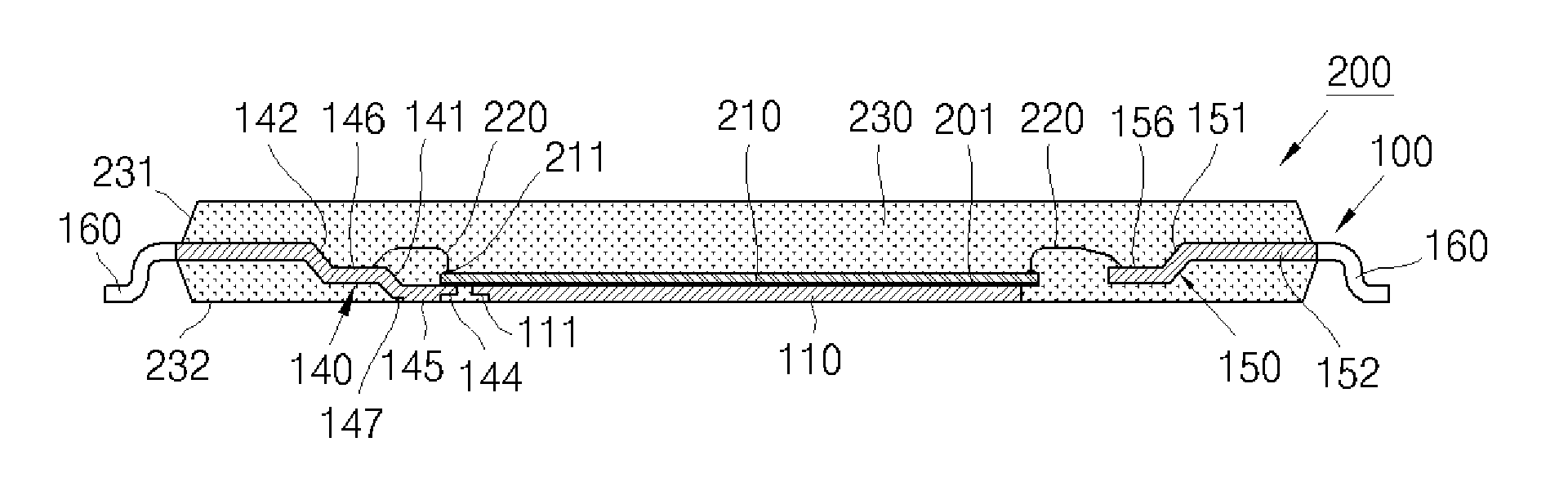
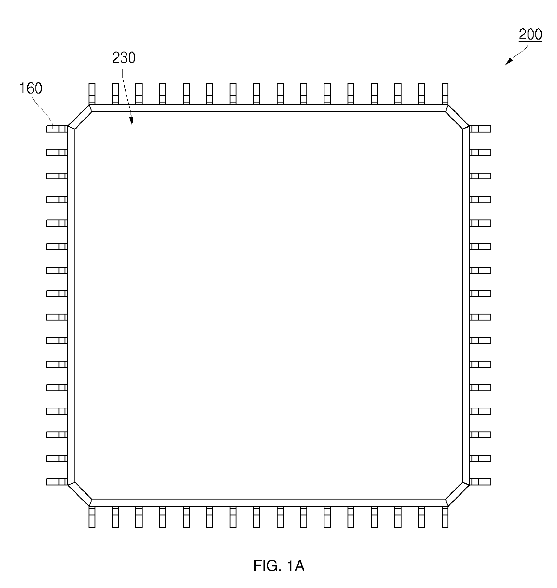
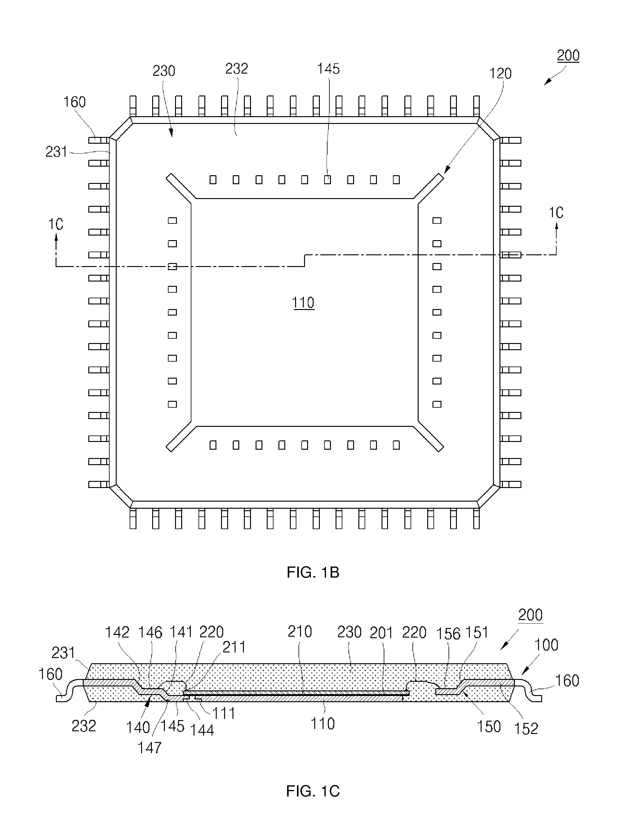
[0042]Referring now to the drawings wherein the showings are for purposes of illustrating one embodiment of the present invention only, and not for purposes of limiting the same, FIGS. 1A-1C depict a semiconductor package 200 constructed in accordance with the present invention. The leadframe 100 integrated into the semiconductor package 200 is shown in its unsingulated state in FIG. 1D.

[0043]Referring now to FIGS. 1A-1D, the leadframe 100 comprises a generally quadrangular (e.g., square) die pad 110 which defines four peripheral edge segments. As best seen in FIGS. 1C and 1D, the die pad 110 of the leadframe 100 is not of uniform thickness. Rather, formed in a peripheral portion of the bottom surface of the die pad 110 is a half-etched portion 111. More particularly, the half-etched portion 111 is segregated into four segments, with each of these segments extending along a respective one of peripheral edge segments of the die pad 110 and between a respective pair of tie bars 120 of...

second embodiment

[0071]Referring now to FIGS. 4A-4C, there is shown a semiconductor package 400 constructed in accordance with the present invention. The leadframe 300 integrated into the semiconductor package 400 is shown in its unsingulated state in FIG. 4D.

[0072]Referring now to FIGS. 4A-4D, the leadframe 300 comprises a generally quadrangular (e.g., square) die pad 310 which defines four peripheral edge segments. As best seen in FIGS. 4C and 4D, the die pad 310 of the leadframe 300 is not of uniform thickness. Rather, formed in a peripheral portion of the bottom surface of the die pad 310 is a half-etched portion 311. More particularly, the half-etched portion 311 is segregated into four segments, with each of these segments extending along a respective one of peripheral edge segments of the die pad 310 and between a respective pair of tie bars 320 of the leadframe 300 which are described in more detail below. Though FIG. 4D is a top plan view of the leadframe 300, the half-etched portion 311 in...

third embodiment

[0096]Referring now to FIGS. 5A-5C, there is shown a semiconductor package 400′ constructed in accordance with the present invention. The leadframe 300′ integrated into the semiconductor package 400′ is shown in its unsingulated state in FIG. 5D. The semiconductor package 400′ bears substantial similarity to the semiconductor package 400 described above. Thus, only the distinctions between the semiconductor packages 400, 400′ will be highlighted below. It should be noted that the common structural features of the semiconductor packages 400, 400′ are identified by the same reference numbers in FIGS. 4A-4D and 5A-5D, with those reference numbers used in conjunction with the semiconductor package 400′ in FIGS. 5A-5D being accompanied by an apostrophe.

[0097]The leadframe 300′ differs from the leadframe 300 by virtue of its inclusion of a plurality of support bars 341′ which are integrally connected to and extend between the die pad 310′ and the land connecting bar 340′. In this regard, ...


PUM


Abstract

In accordance with the present invention, there is provided a semiconductor package (e.g., a QFP package) including a uniquely configured leadframe sized and configured to maximize the available number of exposed leads in the semiconductor package. More particularly, the semiconductor package of the present invention includes a generally planar die pad or die paddle defining multiple peripheral edge segments. In addition, the semiconductor package includes a plurality of leads. Some of these leads include exposed bottom surface portions which are provided in at least one row or ring which at least partially circumvents the die pad, with other leads including portions which protrude from respective side surfaces of a package body of the semiconductor package. Connected to the top surface of the die pad is at least one semiconductor die which is electrically connected to at least some of the leads. At least portions of the die pad, the leads, and the semiconductor die are encapsulated by the package body, with at least portions of the bottom surfaces of the die paddle and some of the leads being exposed in a common exterior surface of the package body.

Description

CROSS-REFERENCE TO RELATED APPLICATIONS[0001]Not ApplicableSTATEMENT RE: FEDERALLY SPONSORED RESEARCH / DEVELOPMENT[0002]Not ApplicableBACKGROUND OF THE INVENTION[0003]1. Field of the Invention[0004]The present invention relates generally to integrated circuit package technology and, more particularly, to an increased capacity QFP semiconductor package which includes exposed leads and an exposed die pad on the bottom surface of the package body thereof, and additional leads which protrude from side surfaces of the package body.[0005]2. Description of the Related Art[0006]Semiconductor dies are conventionally enclosed in plastic packages that provide protection from hostile environments and enable electrical interconnection between the semiconductor die and an underlying substrate such as a printed circuit board (PCB) or motherboard. The elements of such a package include a metal leadframe, an integrated circuit or semiconductor die, bonding material to attach the semiconductor die to ...

Claims


Application Information

Patent Timeline
IPC IPC(8): H01L23/495
CPCH01L23/49541H01L23/49548H01L23/49551H01L25/105H01L23/3128H01L23/3107H01L2224/32225H01L25/03H01L2224/32245H01L2224/48091H01L2224/48247H01L2224/48465H01L2225/1029H01L2225/1058H01L2924/01078H01L2924/01079H01L2924/15311H01L24/48H01L2224/92247H01L2224/73265H01L2224/48227H01L2224/32145H01L2924/00014H01L2924/00H01L2924/00012H01L24/73H01L2924/14H01L2924/181H01L2224/05554H01L2224/49109H01L2924/10162H01L24/49H01L2924/18301H01L2224/45099H01L2224/45015H01L2924/207
Inventor KIM, GI JEONGKIM, WAN JONG
Owner AMKOR TECH SINGAPORE HLDG PTE LTD
Why Eureka
Try Eureka