Semiconductor device with increased I/O leadframe including power bars

a technology of i/o leadframe and power bar, which is applied in the direction of semiconductor devices, semiconductor/solid-state device details, electrical apparatus, etc., can solve the problems of increasing the overall size of qfp packages, further limiting the number of input/output (i/o's) which may be included therein, and conventional leadframe structures as currently known and integrated into existing qfp packages often prove unsatisfactory, so as to achieve the effect of effectively electrically

Active Publication Date: 2013-11-05
AMKOR TECH SINGAPORE HLDG PTE LTD
View PDF453 Cites 20 Cited by
  • Summary
  • Abstract
  • Description
  • Claims
  • Application Information

AI Technical Summary

Benefits of technology

[0014]In accordance with the present invention, there is provided a semiconductor device or semiconductor package (e.g., a QFP package) including a uniquely configured leadframe sized and configured to maximize the available number of exposed leads in the semiconductor package, and further to provide one or more power bars in the semiconductor package. More particularly, the semiconductor package of the present invention includes a generally planar die paddle or die pad defining multiple peripheral edge segments. In addition, the semiconductor package includes a plurality of leads. Some of these leads include exposed bottom surface portions which are provided in at least two concentric rows or rings which at least partially circumvent the die pad, with other leads including portions which protrude from respective side surfaces of a package body of the semiconductor package. Connected to the top surface of the die pad is at least one semiconductor die which is electrically connected to at least some of the leads. At least portions of the die pad, the power bars, leads, and the semiconductor die are encapsulated by the package body, with at least portions of the bottom surfaces of the die pad and some of the leads being exposed in a common exterior surface of the package body. The bottom surface(s) of the power bar(s) may also be exposed in such common exterior surface of the package body, or the power bar(s) may be completely covered by the package body. The leadframe of the semiconductor package is fabricated in accordance with standard, low-cost forming techniques. In accordance with the present invention, sawing, punching, etching, or other material removal processes may be completed during the fabrication of the semiconductor package to effectively electrically isolate the power bars and various leads from each other within the semiconductor package. The semiconductor package of the present invention may include one or more internal semiconductor dies, depending on functional requirements.

Problems solved by technology

One of the deficiencies of currently known QFP packages is attributable to the length at which the leads protrude from the sides of the package body, such protrusion length resulting in an increase in the overall size of the QFP package and further limiting the number of inputs / outputs (I / O's) which may be included therein.
In view of this need, conventional leadframe structures as currently known and integrated into existing QFP packages often prove to be unsatisfactory.
Another deficiency of existing QFP packages is the absence of power bars which are often needed for power supply or ground connection.
However, in currently known leadframe designs for QFP packages, the power bars and / or ground rings are often not connected to other support structures of the leadframe and thus “float,” thus necessitating that they be fixed to the remainder of the leadframe through the use of, for example, lead lock tape.
As will be recognized, this use of lead lock tape renders the power bars and / or ground rings structurally unstable, with such instability often leading to poor flatness relative to the signal leads.
Additionally, the inclusion of power bars in currently known leadframe configurations for QFP packages often carries a significant penalty attributable to the resultant increase in size of the leadframe, and hence the QFP package including the same.
However, the circuit boards integrated into these types of semiconductor packages are expensive and typically exhibit poor heat sink and electrical performance characteristics in comparison to semiconductor packages employing leadframes.
Such a structure is difficult to achieve in a semiconductor package employing a circuit board.

Method used


Image

  • Semiconductor device with increased I/O leadframe including power bars
  • Semiconductor device with increased I/O leadframe including power bars
  • Semiconductor device with increased I/O leadframe including power bars

Examples


first embodiment

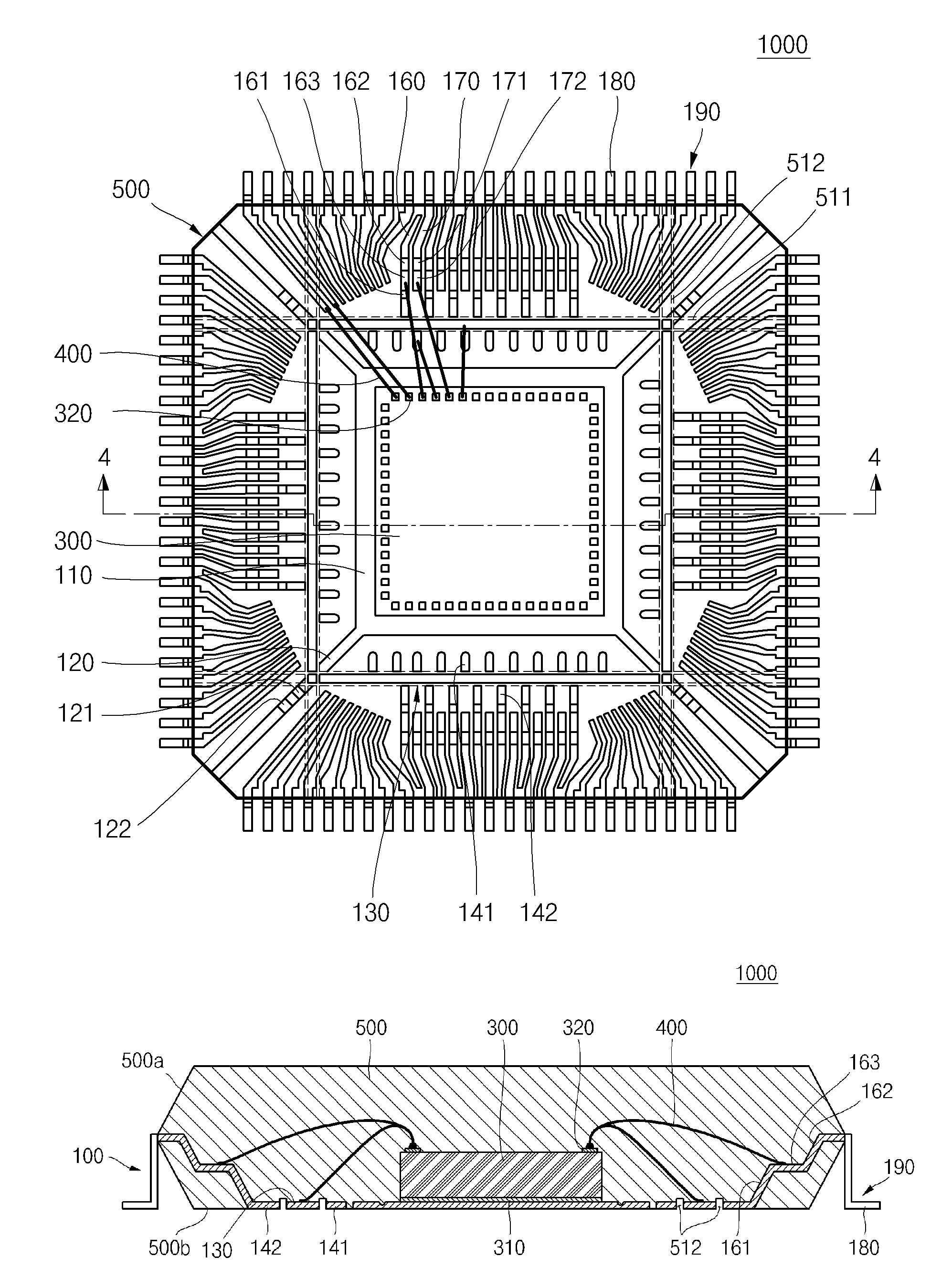
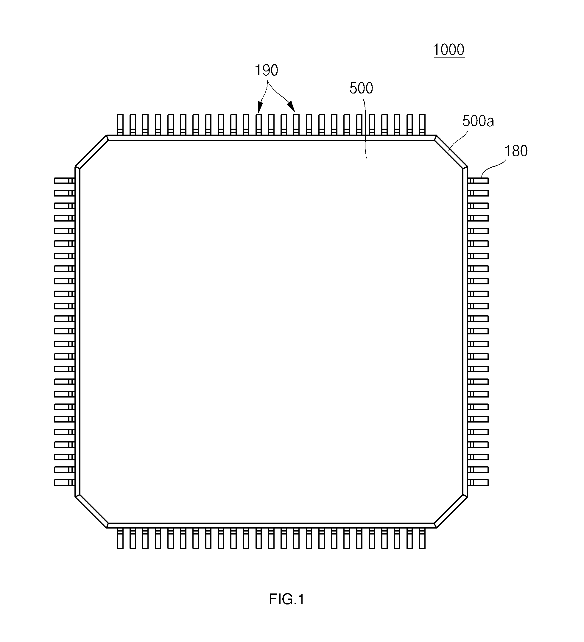
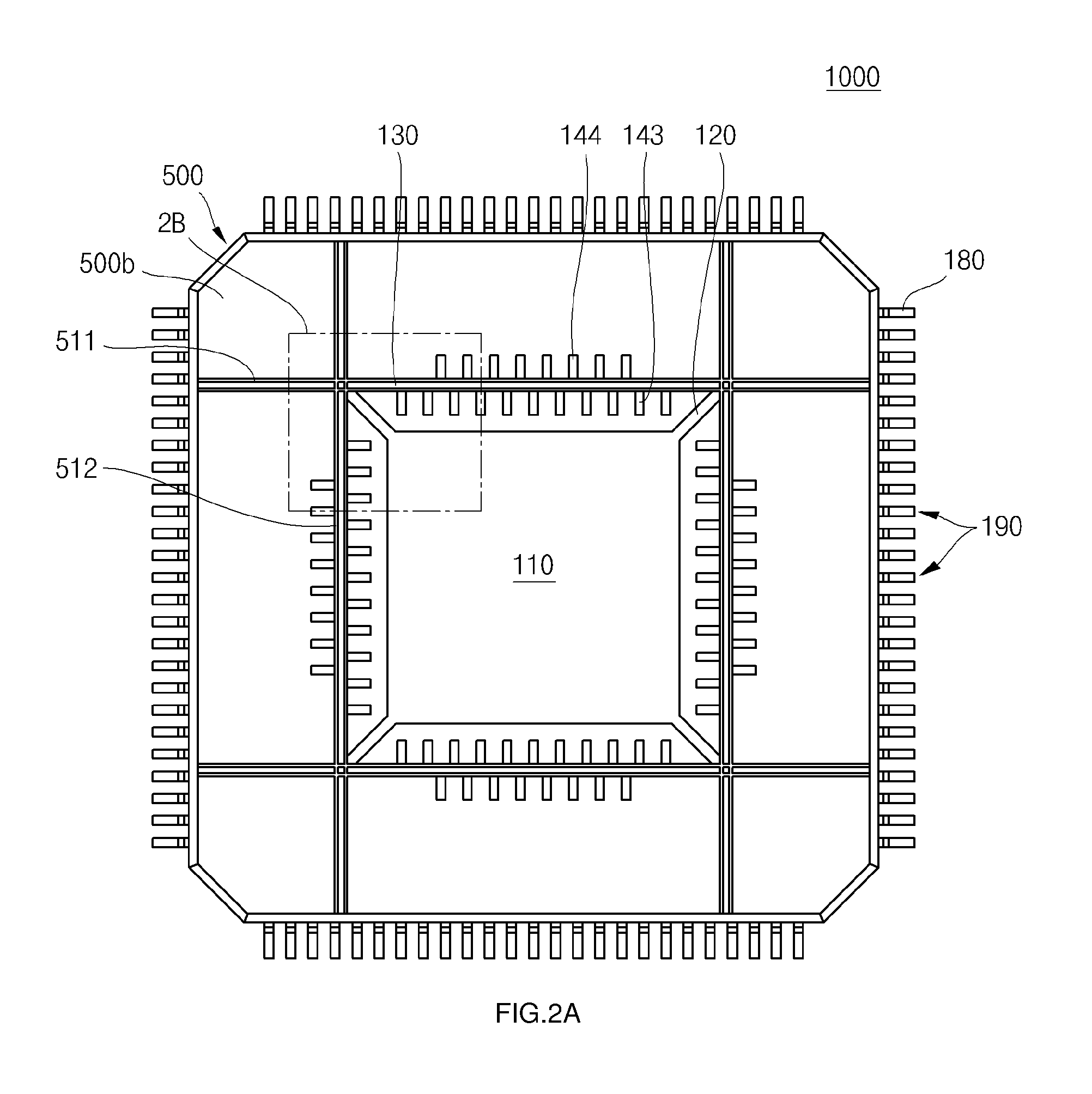
[0026]Referring now to the drawings wherein the showings are for purposes of illustrating one embodiment of the present invention only, and not for purposes of limiting the same, FIGS. 1-4 depict a semiconductor package 1000 constructed in accordance with the present invention. Integrated into the semiconductor package 1000 is a leadframe 100, the structural attributes of which will be described in more detail below. In FIGS. 7B, 9B and 10B, the leadframe 100 is shown in its original, unsingulated state. In FIGS. 3 and 12B, the leadframe 100 is shown in its post-singulation, completed state.

[0027]The leadframe 100 of the semiconductor package 1000 comprises a generally quadrangular (e.g., square) die pad 110 which defines four peripheral edge segments. Integrally connected to the die pad 110 is a plurality of tie bars 120. More particularly, the leadframe 100 includes four tie bars 120 which extend diagonally from respective ones of the four corner regions defined by the die pad 110...

second embodiment

[0060]Referring now to FIG. 5, there is shown in cross-section a semiconductor package 2000 constructed in accordance with the present invention. The semiconductor package 2000 is substantially similar to the above-described semiconductor package 1000, with only the distinctions between the semiconductor packages 2000, 1000 being described below.

[0061]The sole distinction between the semiconductor packages 2000, 1000 lies in the bottom surfaces of the power bars 230 included in the semiconductor package 2000 being half-etched. As a result of such half-etching, the bottom surfaces of the power bars 230 are covered by the package body 500, unlike those of the power bars 130 of the semiconductor package 1000 which, as indicated above, are exposed in and substantially flush with the bottom surface 500b of the package body 500. Since the power bars 230 in the semiconductor package 2000 are not exposed to the outside, higher electrical reliability is achieved in the semiconductor package ...


PUM


Abstract

A semiconductor device or semiconductor package (e.g., a QFP package) including a uniquely configured leadframe sized and configured to maximize the available number of exposed leads in the semiconductor package, and further to provide one or more power bars in the semiconductor package. More particularly, the semiconductor package of the present invention includes a generally planar die paddle or die pad defining multiple peripheral edge segments. In addition, the semiconductor package includes a plurality of leads. Some of these leads include exposed bottom surface portions which are provided in at least two concentric rows or rings which at least partially circumvent the die pad, with other leads including portions which protrude from respective side surfaces of a package body of the semiconductor package. Connected to the top surface of the die pad is at least one semiconductor die which is electrically connected to at least some of the leads. At least portions of the die pad, the power bars, leads, and the semiconductor die are encapsulated by the package body, with at least portions of the bottom surfaces of the die pad and some of the leads being exposed in a common exterior surface of the package body. The bottom surface(s) of the power bar(s) may also be exposed in such common exterior surface of the package body, or the power bar(s) may be completely covered by the package body.

Description

CROSS-REFERENCE TO RELATED APPLICATIONS[0001]Not ApplicableSTATEMENT RE: FEDERALLY SPONSORED RESEARCH / DEVELOPMENT[0002]Not ApplicableBACKGROUND OF THE INVENTION[0003]1. Field of the Invention[0004]The present invention relates generally to integrated circuit package technology and, more particularly, to an increased capacity QFP semiconductor package which includes one or more internal power bars, exposed leads and an exposed die pad on the bottom surface of the package body thereof, and additional leads which protrude from side surfaces of the package body.[0005]2. Description of the Related Art[0006]Semiconductor dies are conventionally enclosed in plastic packages that provide protection from hostile environments and enable electrical interconnection between the semiconductor die and an underlying substrate such as a printed circuit board (PCB) or motherboard. The elements of such a package include a metal leadframe, an integrated circuit or semiconductor die, bonding material to...

Claims


Application Information

Patent Timeline
Patent Type & Authority Patents(United States)
IPC IPC(8): H01L23/52
CPCH01L23/49541H01L23/49551H01L23/3107H01L2224/48247H01L2224/48465H01L2224/49109H01L2224/73265H01L2224/92247H01L2924/00H01L2924/181H01L2224/05554H01L2224/49433H01L2924/00012
Inventor KIM, WAN JONGDO, YOUNG TAKCHO, BYONG WOO
Owner AMKOR TECH SINGAPORE HLDG PTE LTD
Why Eureka
Try Eureka